LB1998 데이터 시트보기 (PDF) - SANYO -> Panasonic
부품명
상세내역
제조사
LB1998 Datasheet PDF : 9 Pages
| |||
LB1998
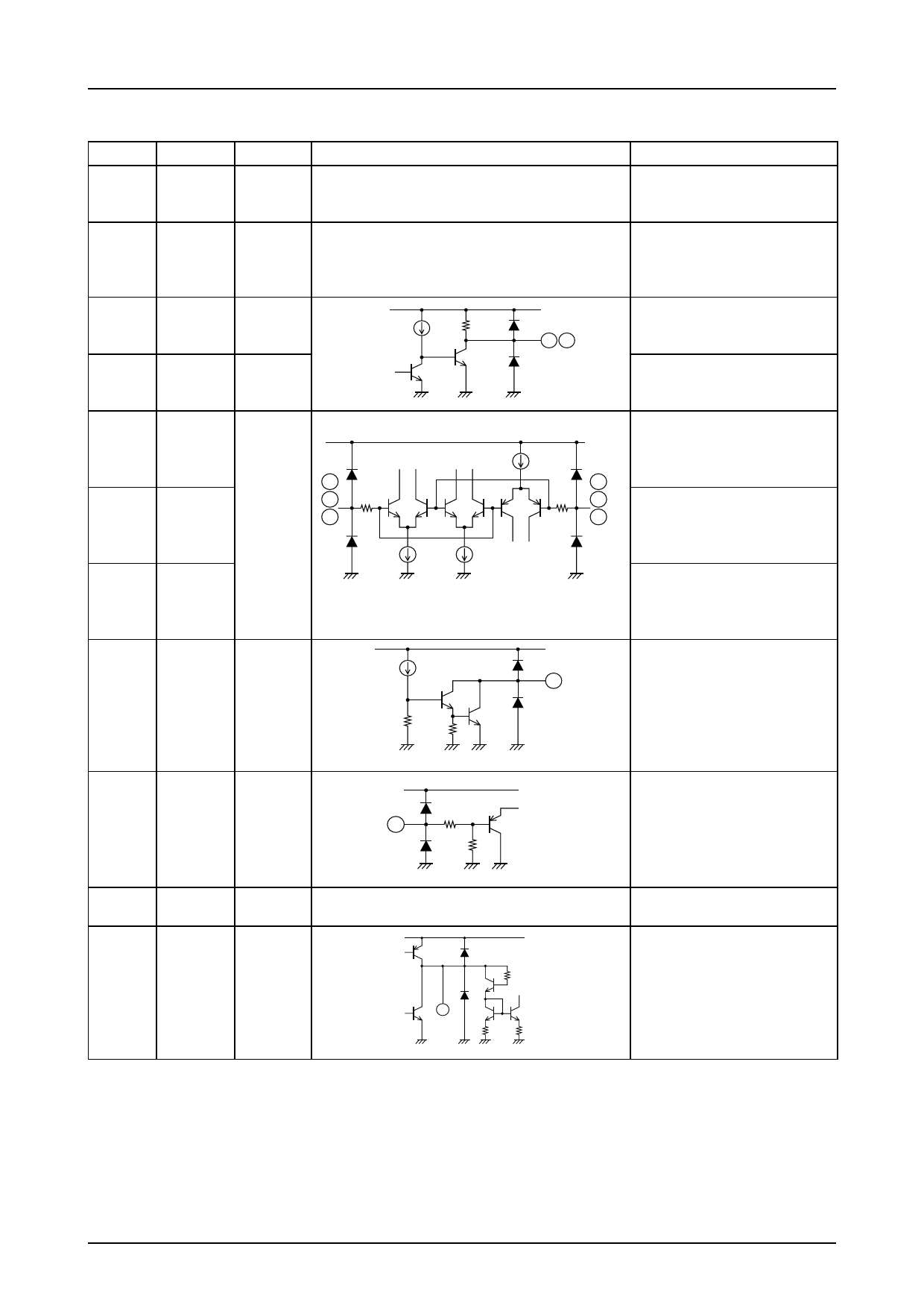
Pin Descriptions
Pin number Pin name Pin voltage
Equivalent circuit
Pin function
19
VCC2
4V to 13.6V
Source side predrive voltage and
constant current control amplifier
voltage supply pin
17
VCC1
4V to 6V
9
RS
Power supply pin for all circuits
except output transistors, source
predriver, and low current control
amplifier
100µA
10 kΩ
VCC1
89
Reverse detector pin
Forward rotation: High
Reverse rotation: Low
8
FG
15
UIN1
16
UIN2
11
13 200Ω
13
14
VIN1
VIN2
1.2V to
15
VCC1–1V
25µA
11
WIN1
12
WIN2
75µA
1 Hall or 3 Hall element waveform
Schmitt comparator combined
A11196
output
U phase Hall element input and
VCC1 reverse detector U phase Schmitt
25µA
comparator input pin
12
Logic High indicates UIN1 > UIN2.
14 V phase Hall element input and
200Ω 16
reverse detector V phase Schmitt
comparator input pin
25µA
Logic High indicates VIN1 > VIN2.
A11197
W phase Hall element input and
reverse detector W phase Schmitt
comparator input pin
Logic High indicates WIN1 > WIN2.
VCC1
Hall element lower side bias voltage
supply pin
10
10
VH
30 kΩ
2 kΩ
6
S/S
0V to WCC1
75 kΩ
6
50 kΩ
A11198
VCC1
When this pin is at 0.7V or lower, or
when it is open, all circuits are
inactive. When driving motor, set
this pin to 2V or higher.
5
SIG GND
24
FC
A11199
VCC1
2 kΩ
24
20 kΩ
5 kΩ
A11200
GND pin for all circuits except
output
Control loop frequency compensa-
tor pin. Connecting a capacitor
between this pin and GND prevents
closed loop oscillation in current
limiting circuitry.
Continued on next page
No. 5979-7/9
Share Link: 