MC141515 데이터 시트보기 (PDF) - Motorola => Freescale
부품명
상세내역
제조사
MC141515 Datasheet PDF : 15 Pages
| |||
PIN DESCRIPTIONS
VDD AND VSS
Power is supplied to the driver using these two pins. VDD is power
and VSS is ground.
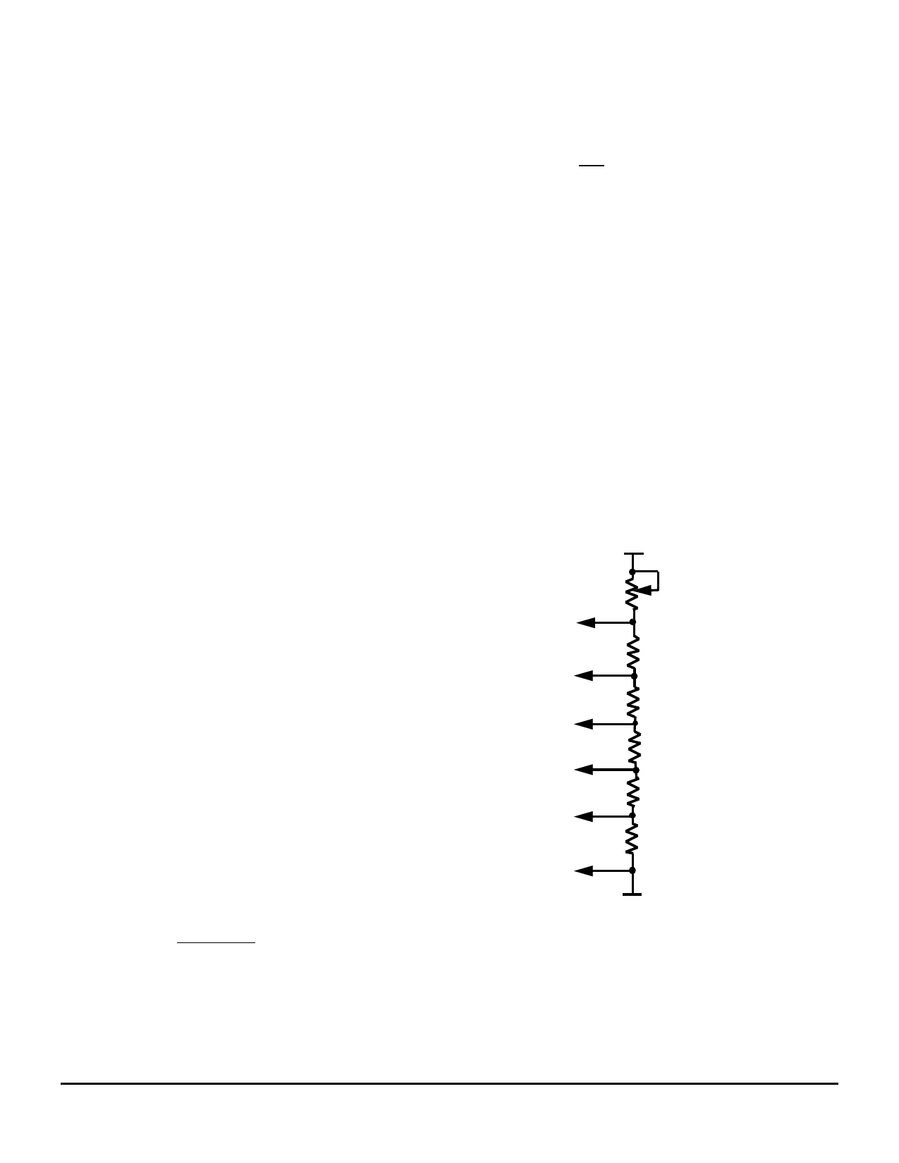
V<1>, V<5>, V<6>
These are the levels of voltage generated from an external volt-
ages divider (Fig. 1).
DOFF
This is an output from MC68HC05L11 to signal the backplane
driver to turn off LCD. If this signal is clear, the backplane driver will sup-
ply LCD with driving signal. If this signal is set, the backplane driver out-
puts will be high-impedanced and LCD display is disabled.
FRM
A periodic active high input to the backplane driver for frame tim-
ing synchronization which is connected to FRM of MC68HC05L11.
BPCLK
A periodic output from MC68HC05L11 to backplane driver for tim-
ing synchronization. The signal will affect the refreshing time of LCD
display.
FMC
This is an output pin of backplane driver which is connected to the
FRM of the next backplane driver in case of cascading.
M
This pin is for synchronization between the display driver. When
MGEN is set, it will generate an M signal for synchronization. When
MGEN is clear, it becomes an input pin and expecting a M signal from
other device.
MGEN
An input which is used for program the M pin as an input or output.
If MGEN is logic high, M acts as an output. If MGEN is logic low, M
becomes an input.
COM 0 - 79
These are the high voltage outputs of the backplane driver which
are connected to set of common lines of any LCD panel.
OPERATION OF LCD DRIVER
INTRODUCTION
The LCD backplane driver can support multiplex ratio of a LCD
system up to 146 and cascading of more than one driver for expansion
is possible. It can be set from 1:5 bias (for 16 mux) to 1:13 bias (for 146
mux), by the voltage divider ratio of Fig.1. The ratio of bias or the con-
trast ratio (a) is defined as
1:
4 x R1 + R2
R1
=1:a
As the multiplex ratio changes, the ratio of bias has to be changed
accordingly. The ratio of bias relates to the multiplex ratio as
a = mux + 1
To set up a multiplex ratio, please refer to MC68HC05L11 techni-
cal data Section 10.6.2.
VOLTAGES SELECTOR consists of switching circuit to select appropri-
ate voltage levels from external voltage divider. (See Fig. 1).
80-BIT SHIFT REGISTER samples the FRM at the falling edge of
BPCLK and shifts the sample to the left 80 times before exports to the
next backplane driver through FMC.
HIGH VOLTAGE DRIVERS ARRAY is a row of high voltage drivers
connecting to segment lines of any LCD panel. The output waveform of
the high voltage driver is shown as Com(1) and Com(2)are shown in
Figure 2.
POWER UP SYNCHRONIZATION is activated upon the receipt the first
M pulse. The M pin of the backplane driver will act as an input when
MGEN is connected to Low. When MGEN is Set, this backplane driver
will be the master of the synchronization system. M pin will then supply
a periodic signal for all LCD drivers.
VLCD
V<1>
R1
V<6>
R1
V<3>
R2
V<4>
R1
V<5>
R1
V<2>
Contrast Control
VSS
Figure 1. External Voltage Divider
MOTOROLA
MC141512 • MC141515
3–41
Share Link: 