NCV8705(2014) 데이터 시트보기 (PDF) - ON Semiconductor
부품명
상세내역
제조사
NCV8705
(Rev.:2014)
(Rev.:2014)
ON Semiconductor

NCV8705 Datasheet PDF : 20 Pages
| |||
NCV8705
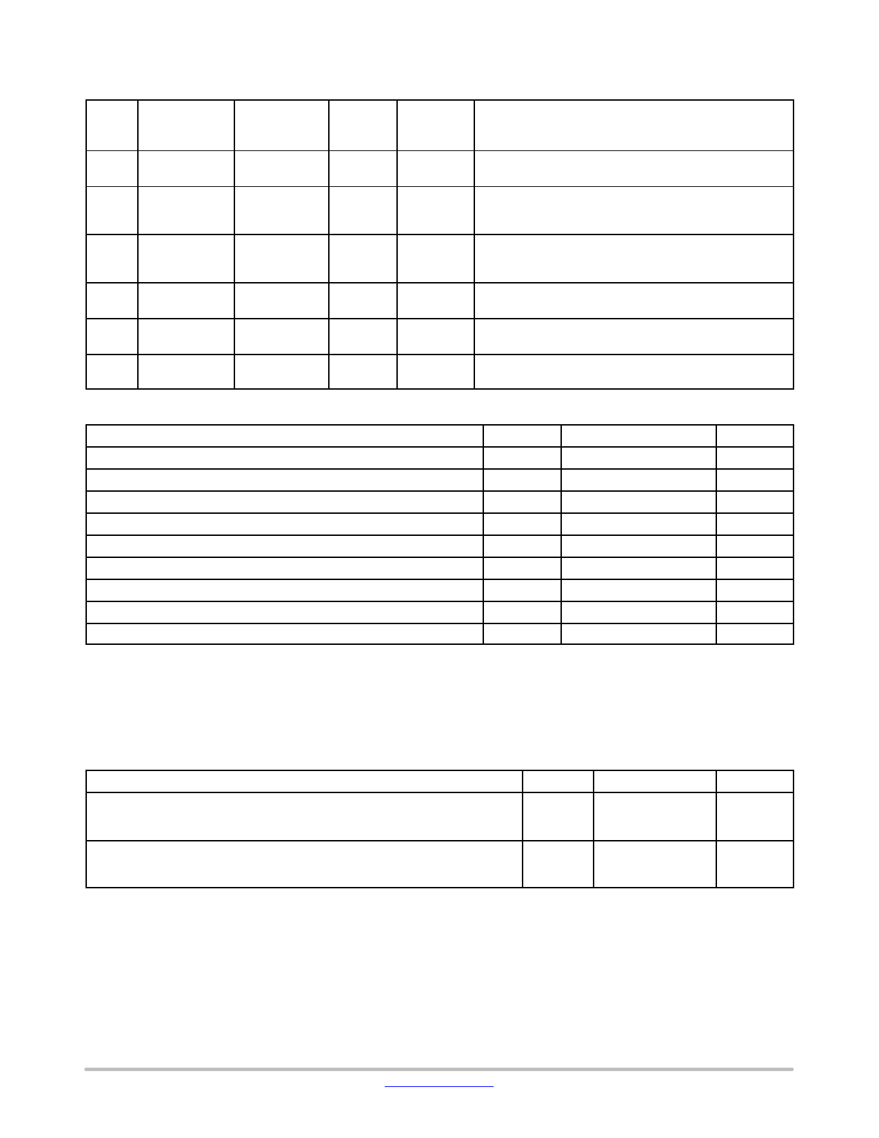
Table 1. PIN FUNCTION DESCRIPTION
Pin No.
Pin Name −
Fixed
Pin Name −
Adjustable
Description
1
OUT
OUT
Regulated output voltage pin. A small 1 mF ceramic capacitor is needed from this pin to
ground to assure stability.
2
N/C
ADJ
Feedback pin for set−up output voltage. Use resistor divider for voltage selection.
3
GND
GND
Power supply ground. Expose pad must be tied with GND pin. Soldered to the copper
plane allows for effective heat dissipation.
4
EN
EN
Enable pin. Driving EN over 0.9 V turns on the regulator. Driving EN below 0.4 V puts
the regulator into shutdown mode.
5
N/C
N/C
Not connected. This pin can be tied to ground to improve thermal dissipation.
6
IN
IN
Input pin. A small capacitor is needed from this pin to ground to assure stability.
Table 2. ABSOLUTE MAXIMUM RATINGS
Rating
Symbol
Value
Unit
Input Voltage (Note 1)
VIN
−0.3 V to 6 V
V
Output Voltage
VOUT
−0.3 V to VIN + 0.3 V
V
Enable Input
VEN
−0.3 V to VIN + 0.3 V
V
Adjustable Input
VADJ
−0.3 V to VIN + 0.3 V
V
Output Short Circuit Duration
tSC
Indefinite
s
Maximum Junction Temperature
TJ(MAX)
125
°C
Storage Temperature
TSTG
−55 to 150
°C
ESD Capability, Human Body Model (Note 2)
ESDHBM
2000
V
ESD Capability, Machine Model (Note 2)
ESDMM
200
V
Stresses exceeding those listed in the Maximum Ratings table may damage the device. If any of these limits are exceeded, device functionality
should not be assumed, damage may occur and reliability may be affected.
1. Refer to ELECTRICAL CHARACTERISTICS and APPLICATION INFORMATION for Safe Operating Area.
2. This device series incorporates ESD protection and is tested by the following methods:
ESD Human Body Model tested per AEC−Q100−002 (EIA/JESD22−A114)
ESD Machine Model tested per AEC−Q100−003 (EIA/JESD22−A115)
Latchup Current Maximum Rating tested per JEDEC standard: JESD78.
Table 3. THERMAL CHARACTERISTICS (Note 3)
Rating
Thermal Characteristics, WDFN6 2x2 mm
Thermal Resistance, Junction−to−Air
Thermal Resistance Parameter, Junction−to−Board
3. Single component mounted on 1 oz, FR 4 PCB with 645 mm2 Cu area.
Symbol
qJA
YJB
Value
116.5
30
Unit
°C/W
www.onsemi.com
3
Share Link: