AS7C1026 데이터 시트보기 (PDF) - Alliance Semiconductor
부품명
상세내역
제조사
AS7C1026 Datasheet PDF : 10 Pages
| |||
AS7C1026
AS7C31026
®
Functional description
The AS7C1026 and AS7C31026 are high-performance CMOS 1,048,576-bit Static Random Access Memory (SRAM) devices
organized as 65,536 words x 16 bits. They are designed for memory applications where fast data access, low power, and simple
interfacing are desired.
Equal address access and cycle times (tAA, tRC, tWC) of 12/15/20 ns with output enable access times (tOE) of 6,7,8 ns are ideal
for high-performance applications.
When CE is high the devices enter stanby mode. The AS7C1026 is guaranteed not to exceed 28 mW power consumption in
CMOS standby mode. The devices also offer 2.0V data retention.
A write cycle is accomplished by asserting write enable (WE) and chip enable (CE). Data on the input pins I/O0–I/O15 is
written on the rising edge of WE (write cycle 1) or CE (write cycle 2). To avoid bus contention, external devices should drive I/
O pins only after outputs have been disabled with output enable (OE) or write enable (WE).
A read cycle is accomplished by asserting output enable (OE) and chip enable (CE), with write enable (WE) high. the chips drive
I/O pins with the data word referenced by the input address. When either chip enable or output enable is inactive, or write
enable is active, output drivers stay in high-impedance mode.
The devices provide multiple center power and ground pins, and separate byte enable controls, allowing individual bytes to be
written and read. LB controls the lower bits, I/O0–I/O7, and UB controls the higher bits, I/O8–I/O15.
All chip inputs and outputs are TTL-compatible, and operation is from a single 5V supply (AS7C1026) or 3.3V supply
(AS7C31026). the device is packaged in common industry standard packages. Chip scale BGA packaging, easy to use in
manufacturing, provides the smallest possible footprint. This 48-ball JEDEC-registered package has a ball pitch of 0.75 mm and
external dimensions of 8 mm × 6 mm.
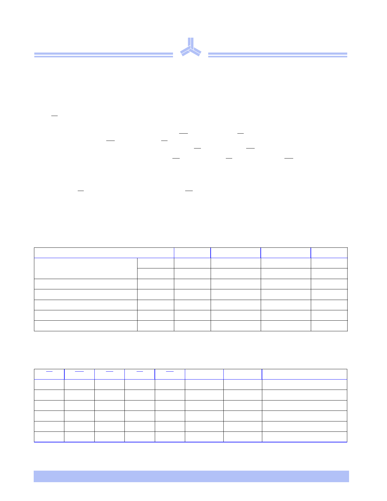
Absolute maximum ratings
Parameter
Symbol
Min
Max
Unit
Voltage on VCC relative to GND
AS7C1026
Vt1
AS7C31026
Vt1
–0.50
–0.50
+7.0
+5.0
V
V
Voltage on any pin relative to GND
Vt2
–0.50
VCC +0.50
V
Power dissipation
Storage temperature (plastic)
Ambient temperature with VCC applied
PD
–
Tstg
–65
Tbias
–55
1.0
W
+150
°C
+125
°C
DC current into outputs (low)
IOUT
–
20
mA
Note: Stresses greater than those listed under Absolute Maximum Ratings may cause permanent damage to the device. This is a stress rating only and functional
operation of the device at these or any other conditions outside those indicated in the operational sections of this specification is not implied. Exposure to
absolute maximum rating conditions for extended periods may affect reliability.
Truth table
CE
WE
OE
LB
UB I/O0–I/O7 I/O8–I/O15
Mode
H
X
X
X
X
High Z
High Z
Standby (ISB), ISBI)
L
H
L
L
H
DOUT
High Z
Read I/O0–I/O7 (ICC)
L
H
L
H
L
High Z
DOUT
Read I/O8–I/O15 (ICC)
L
H
L
L
L
DOUT
DOUT
Read I/O0–I/O15 (ICC)
L
L
X
L
L
DIN
DIN
Write I/O0–I/O15 (ICC)
L
L
X
L
H
DIN
High Z
Write I/O0–I/O7 (ICC)
3/23/01; v.1.0
Alliance Semiconductor
P. 2 of 10
Share Link: 