PI74FCT162500T 데이터 시트보기 (PDF) - Pericom Semiconductor
부품명
상세내역
제조사
PI74FCT162500T Datasheet PDF : 6 Pages
| |||
PI74FCT16500/162500T
PI74FCT16500T 12345678901234567890123456789012123456789012345678901234567890121234567890123456789011823-4B56I7T890R12E12G345I6S78T90E12R34E56D789T01R234A56N78S90C12E12I3V456E78R90S12
PI74FCT162500T
1122334455667788990011223344556677889900112233445566778899001122112233445566778899001122334455667788990011223344556677889900112211223344556677889900112233445566778899001122334455667788990011221122334455667788990011223344556677889900112233445566778899001122112233445566778899001122
Fast CMOS 18-Bit
Registered Transceivers
Product Description:
Product Features:
Common Features:5
• PI74FCT16500TandPI74FCT162500Tarehigh-speed,
low power devices with high current drive.
• VCC =5V±10%
• Hysteresis on all inputs
• Packages available:
– 56-pin 240 mil wide plastic TSSOP (A)
– 56-pin 300 mil wide plastic SSOP (V)
PI74FCT16500T Features:
• High output drive: IOH = –32 mA; IOL = 64 mA
• Power off disable outputs permit “live insertion”
• Typical VOLP (Output Ground Bounce) < 1.0V
at VCC = 5V, TA = 25°C
PI74FCT162500T Features:
• Balanced output drivers: ±24 mA
• Reduced system switching noise
• Typical VOLP (Output Ground Bounce) < 0.6V
at VCC = 5V, TA = 25°C
Pericom Semiconductor’s PI74FCT series of logic circuits are pro-
duced in the Company’s advanced 0.8 micron CMOS technology,
achieving industry leading speed grades.
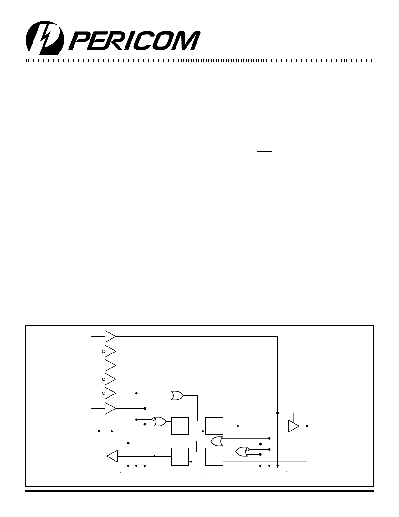
The PI74FCT16500T and PI74FCT162500T are 18-bit registered bus
transceivers designed with D-type latches and flip-flops to allow
data flow in transparent, latched, and clocked modes. The Output
Enable (OEAB and OEBA), Latch Enable (LEAB and LEBA) and
Clock (CLKAB and CLKBA) inputs control the data flow in each
direction. When LEAB is HIGH, the device operates in transparent
mode for A-to-B data flow. When LEAB is LOW, the A data is latched
if CLKAB is held at a HIGH or LOW logic level. The A bus data is
stored in the latch/flip-flop on the HIGH-to-LOW transition of
CLKAB, if LEAB is LOW. OEAB performs the output enable
function on the B port. Data flow from B port to A port is similar using
OEBA, LEBA and CLKBA. These high-speed, low power devices
offer a flow-through organization for ease of board layout.
The PI74FCT16500T output buffers are designed with a Power-Off
disable allowing “live insertion” of boards when used as backplane
drivers.
The PI74FCT162500T has ±24 mA balanced output drivers. It is
designed with current limiting resistors at its outputs to control the
output edge rate resulting in lower ground bounce and undershoot.
This eliminates the need for external terminating resistors for most
interface applications.
Logic Block Diagram
OEAB
CLKBA
LEBA
OEBA
CLKAB
LEAB
A1
C
C
D
D
C
C
D
D
TO 17 OTHER CHANNELS
1
B1
PS2077A 01/15/95
Share Link: 