MT9125AE 데이터 시트보기 (PDF) - Zarlink Semiconductor Inc
부품명
상세내역
제조사
MT9125AE Datasheet PDF : 18 Pages
| |||
Preliminary Information
MT9125
For ST-BUS operation (i.e., when a valid ST-BUS
frame pulse is applied to the F0i input) the bit rate, at
2.048 MHz, is generated internally from the master
clock input at the MCLK pin. The BCLK and ENA
inputs are ignored. Data is latched into the ADPCMi
pin at the three-quarter bit position which occurs at
the second rising edge of MCLK (C4i) within the bit
cell boundary. Output data, on ADPCMo, is made
available at the first falling edge of MCLK (C4i) within
the bit cell boundary. Refer to Figure 13.
ADPCM word placement, within the ST-BUS frame,
is governed by the logic state applied at the ENS
input pin. Referring to Figure 4, when ENS = 0, the
ADPCM words are placed in channel 2 while when
ENS = 1 the ADPCM words are placed in channel 3.
Unlike the PCM octets the ADPCM words never
reside within the ST-BUS channel 0 or 1 timeslots.
PCM Port Operation (DSTi, DSTo, ENB1, ENB2)
The PCM port consists of DSTi, DSTo, ENB1 and
ENB2. PCM port functionality is almost identical for
both ST-BUS and SSI operation, the difference being
from where the BCLK signal is derived and whether
the enable strobes are generated internally or
sourced externally.
Both channels of PCM octets are transferred over
DSTi/DSTo at the bit clock rate during the channel
time defined by the input strobes at ENB1 and ENB2
or by internally generated timeslots.
For ST-BUS operation, (i.e., when a valid ST-BUS
frame pulse is applied to the F0i input) the bit rate, at
2.048 MHz, is generated internally from the master
clock input at the MCLK pin. The BCLK and ENA
inputs are ignored. ST-BUS timeslot assignment is
also generated internally and can be programmed
into channels 0 and 1 or into channels 2 and 3 with
the ENS input pin. Refer to Figure 4. In this mode the
ENB1 and ENB2 inputs are ignored by the device.
The decoded channel timeslots (0 and 1 or 2 and 3)
are made available, along with the 2.048 MHz bit
clock, at EN1, EN2 and C2o for controlling CODEC
devices as shown in the Applications section (refer to
Figures 7 and 11). Data is latched into the DSTi pin
at the three-quarter bit position which occurs at the
second rising edge of MCLK (C4i) within the bit cell
boundary. Output data, on DSTo, is made available
at the first falling edge of MCLK (C4i) within the bit
cell boundary. Refer to Figure 12.
For SSI operation, (i.e., when F0i is tied continuously
to VSS) the bit rate is set by the input clock presented
at the BCLK pin. Data is transferred at the bit clock
rate (BCLK) during the B1 and B2 channels as
defined by input strobes ENB1 and ENB2,
respectively. Note that ENB1 and ENB2 are also
used as the framing inputs for internal operation of
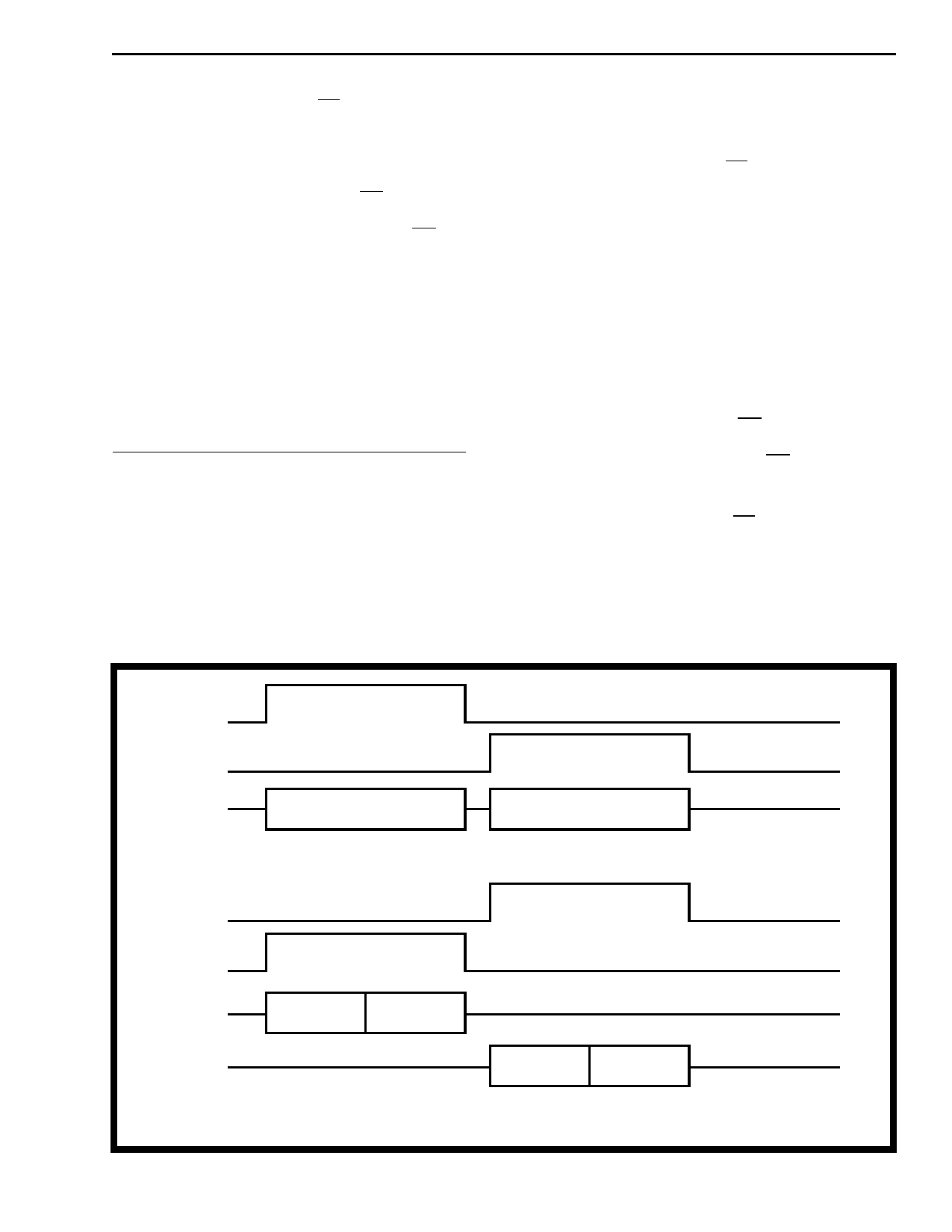
ENB1
ENB2
DSTi/o
8 bits
B1 Channel
8 bits
B2 Channel
ENA
4 bits
4 bits
4 bits
4 bits
B1
B2
ADPCMi/o
B1
B2
Normally ENA is derived from the same strobes which drive the ENB1 or ENB2 inputs. However, as long as ENA
is eight cycles of BCLK length, it may be positioned anywhere within the 8 kHz frame.
Figure 3 - SSI Mode Relative Timing
8-77
Share Link: 