LH28F800SGXX-L10 데이터 시트보기 (PDF) - Sharp Electronics
부품명
상세내역
제조사
LH28F800SGXX-L10 Datasheet PDF : 45 Pages
| |||
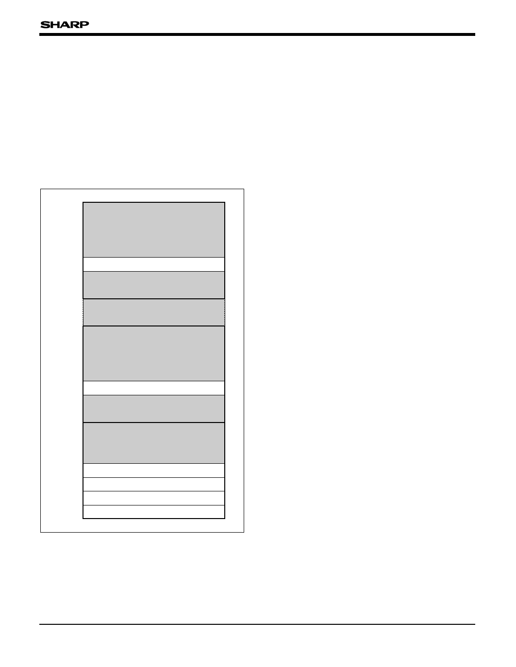
3.5 Read Identifier Codes
The read identifier codes operation outputs the
manufacture code, device code, block lock
configuration codes for each block, and the
permanent lock configuration code (see Fig. 2).
Using the manufacture and device codes, the
system CPU can automatically match the device
with its proper algorithms. The block lock and
permanent lock configuration codes identify locked
and unlocked blocks and permanent lock-bit setting.
7FFFF
78004
78003
78002
78001
78000
Reserved for
Future Implementation
Block 15 Lock Configuration Code
Reserved for
Future Implementation
Block 15
(Blocks 2 through 14)
0FFFF
08004
08003
08002
08001
08000
07FFF
00004
00003
00002
00001
00000
Reserved for
Future Implementation
Block 1 Lock Configuration Code
Reserved for
Future Implementation
Block 1
Reserved for
Future Implementation
Permanent Lock Configuration Code
Block 0 Lock Configuration Code
Device Code
Manufacture Code Block 0
Fig. 2 Device Identifier Code Memory Map
LH28F800SG-L/SGH-L (FOR TSOP, CSP)
3.6 Write
Writing commands to the CUI enable reading of
device data and identifier codes. They also control
inspection and clearing of the status register.
The Block Erase command requires appropriate
command data and an address within the block to
be erased. The Word Write command requires the
command and address of the location to be written.
Set Permanent and Block Lock-Bit commands
require the command and address within the device
(Permanent Lock) or block within the device (Block
Lock) to be locked. The Clear Block Lock-Bits
command requires the command and address
within the device.
The CUI does not occupy an addressable memory
location. It is written when WE# and CE# are
active. The address and data needed to execute a
command are latched on the rising edge of WE# or
CE# (whichever goes high first). Standard
microprocessor write timings are used. Fig. 14 and
Fig. 15 illustrate WE# and CE# controlled write
operations.
4 COMMAND DEFINITIONS
When the VPP ≤ VPPLK, read operations from the
status register, identifier codes, or blocks are
enabled. Placing VPPH1/2/3 on VPP enables
successful block erase, word write and lock-bit
configuration operations.
Device operations are selected by writing specific
commands into the CUI. Table 3 defines these
commands.
-9-
Share Link: 