SR120 데이터 시트보기 (PDF) - Chip Integration Technology Corporation
부품명
상세내역
제조사
SR120 Datasheet PDF : 3 Pages
| |||
SR12 THRU SR120
1A Leaded Type Schottky Barrier Rectifiers
■ Features
• Electrostatic discharge (ESD) test under IEC6100-4-2
standard >16ΚV(SR12~SR16).
standard >10ΚV(SR110~SR120).
• Axial lead type devices for through hole design.
• Low power loss, high efficiency.
• High current capability, low forward voltage drop.
• High surge capability.
• Ultra high-speed switching.
• Silicon epitaxial planar chip, metal silicon junction.
• Suffix "G" indicates Halogen-free part, ex.SR12G.
• Lead-free parts meet environmental standards of
MIL-STD-19500 /228
■ Mechanical data
• Epoxy:UL94-V0 rated flame retardant
• Case : Molded plastic, DO-204AL / DO-41
• Lead : Axial leads, solderable per MIL-STD-202,
Method 208 guranteed
• Polarity : Color band denotes cathode end
• Weight : Approximated 0.33 gram
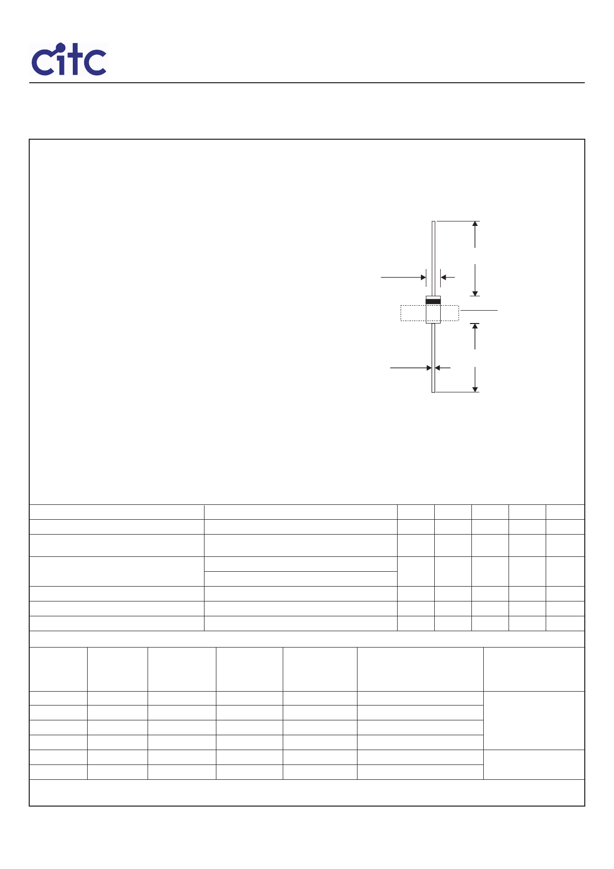
■ Outline
DO-41(DO-204AL)
1.0 (25.4) MIN.
.107 (2.7)
.080 (2.0)
DIA.
.205 (5.2)
Marking code .165 (4.2)
.034 (0.9)
.028 (0.7)
DIA.
1.0 (25.4) MIN.
Dimensions in inches and (millimeters)
■ Maximum ratings and electrical characteristics
Rating at 25OC ambient temperature unless otherwise specified. Single phase, half wave, 60Hz, resistive or inductive load.
For capacitive load, derate current by 20%.
Parameter
Forward rectified current
Forward surge current
Reverse current
Diode junction capacitance
Thermal resistance
Storage temperature
Conditions
Symbol
See Fig.1
IO
8.3ms single half sine-wave superimposed on
rate load (JEDEC method)
IFSM
VR = VRRM TA = 25OC
IR
VR = VRRM TA = 100OC
f=1MHz and applied 4V DC reverse voltage
CJ
Junction to ambient
RθJA
TSTG
MIN.
-55
TYP.
120
88
MAX.
1.0
30
0.5
20
+175
UNIT
A
A
mA
pF
OC/W
OC
Symbol
SR12
SR14
SR16
SR110
SR115
SR120
Max.
repetitive peak
Marking code
reverse voltage
VRRM (V)
SR12
20
SR14
40
SR16
60
SR110
100
SR115
150
SR120
200
Max.
RMS voltage
VRMS (V)
14
28
42
70
105
140
Max. DC
blocking voltage
VR (V)
20
40
60
100
150
200
Max. forward voltage
@1A, TA = 25OC
VF (V)
0.45
0.50
0.70
0.81
0.87
0.90
Operating temperature
TJ (OC)
-50 ~ +150
-50 ~ +175
Document ID : DS-11K98
1
Issued Date : 2010/05/05
Revised Date : 2012/05/31
Revision : C
Share Link: 