MF6 데이터 시트보기 (PDF) - Unspecified
부품명
상세내역
제조사
MF6 Datasheet PDF : 20 Pages
| |||
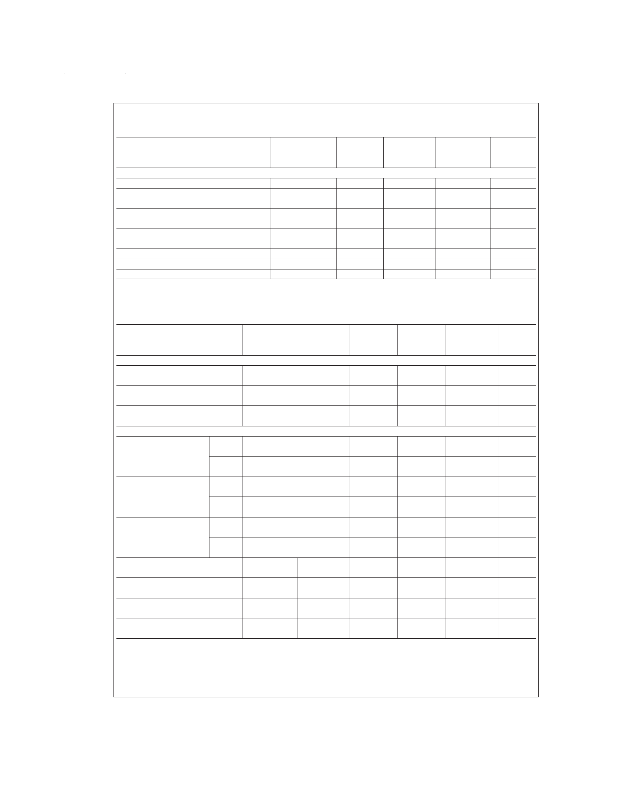
Op Amp Electrical Characteristics (Continued)
Boldface limits apply for TMIN to TMAX; all other limits TA = TJ = 25˚C.
Parameter
Conditions
Typical
(Note 8)
V+ = +2.5V, V− = −2.5V
Input Bias Current
CMRR (Op-Amp #2 Only)
Output Voltage Swing
Maximum Output Short
Circuit Current (Note 6)
Slew Rate
DC Open Loop Gain
Gain Bandwidth Product
Source
Sink
VCM1 = +0.5V,
VCM2 = −0.9V
RL = 10 kΩ
10
60
+1.5
−2.2
24
1.0
6.0
67
1.2
Tested
Limit
(Note 9)
55
+1.3
−1.7
Design
Limit
(Note 10)
+1.1
−1.7
Units
pA
dB
V
mA
V/µs
dB
MHz
Logic Input-Output Electrical Characteristics
(Note 5) The following specifications apply
TMAX; all other limits TA = TJ = 25˚C.
for
V−
=
0V
unless
otherwise
specified.
Boldface
limits
apply
for
TMIN
to
Parameter
Conditions
Typical
Tested
Design
Units
(Note 8)
Limit
Limit
(Note 9)
(Note 10)
TTL CLOCK INPUT, CLK R PIN (Note 7)
Maximum VIL, Logical “0”
Input Voltage
0.8
0.8
V
Minimum VIH, Logical “1”
Input Voltage
2.0
2.0
V
Maximum Leakage Current
L Sh Pin at
2.0
2.0
µA
at CLK R Pin
Mid- Supply
SCHMITT TRIGGER
VT+, Positive Going
Threshold Voltage
Min
V+ = 10V
Max
Min
V+ = 5V
7.0
6.1
8.9
3.5
3.1
6.1
V
8.9
3.1
V
VT−, Negative Going
Threshold Voltage
Max
Min
V+ = 10V
Max
Min
V+ = 5V
4.4
3.0
1.3
3.8
1.5
0.6
4.4
1.3
V
3.8
0.6
V
Hysteresis (VT+ − VT−)
Max
Min
V+ = 10V
Max
Min
V+ = 5V
1.9
4.0
2.3
7.6
2.0
1.2
1.9
2.3
V
7.6
1.2
V
Max
Minimum Logical “1” Output
Voltage (Pin 11)
Io = −10µA
V+ = 10V
V+ = 5V
Maximum Logical “0” Output
Voltage (Pin 11)
Io = 10µA
V+ = 10V
V+ = 5V
Minimum Output Source
CLK R Tied
V+ = 10V
6.0
Current (Pin 11)
to Ground
V+ = 5V
1.5
Maximum Output Sink
CLK R Tied
V+ = 10V
5.0
Current (Pin 11)
to V+
V+ = 5V
1.3
3.8
9.0
4.5
1.0
0.5
3.0
0.75
2.5
0.65
3.8
9.0
V
4.5
1.0
V
0.5
3.0
mA
0.75
2.5
mA
0.65
Note 1: The cutoff frequency of the filter is defined as the frequency where the magnitude response is 3.01 dB less than the DC gain of the filter.
Note 2: For ±5V supplies the dynamic range is referenced to 2.82 Vrms (4V peak) where the wideband noise over a 20 kHz bandwidth is typically 200 µVrms for
the MF6-50 and 250 µVrms for the MF6-100. For ±2.5V supplies the dynamic range is referenced to 1.06 Vrms (1.5V peak) where the wideband noise over a 20 kHz
bandwidth is typically 140 µVrms for both the MF6-50 and the MF6-100.
Note 3: The specifications for the MF6 have been given for a clock frequency (fCLK) of 250 kHz and less. Above this clock frequency the cutoff frequency begins to
deviate from the specified error band of ±1.0% but the filter still maintains its magnitude characteristics. See Application Hints, Section 1.5.
www.national.com
4
Share Link: 