HI1171 데이터 시트보기 (PDF) - Renesas Electronics
부품명
상세내역
제조사
HI1171 Datasheet PDF : 7 Pages
| |||
HI1171
Absolute Maximum Ratings
Thermal Information
Digital Supply Voltage DVDD to DVSS . . . . . . . . . . . . . . . . . . +7.0V
Analog Supply Voltage AVDD to AVSS . . . . . . . . . . . . . . . . . . +7.0V
Input Voltage . . . . . . . . . . . . . . . . . . . . . . . . . . . . . . . . VDD to VSS V
Output Current . . . . . . . . . . . . . . . . . . . . . . . . . . . . . . . 0mA to 15mA
Operating Conditions
Temperature Range. . . . . . . . . . . . . . . . . . . . . . . . . . -40oC to 85oC
Thermal Resistance (Typical, Note 1)
JA (oC/W)
SOIC Package . . . . . . . . . . . . . . . . . . . . . . . . . . . . .
98
Maximum Junction Temperature, Plastic Package . . . . . . . . 150oC
Maximum Storage Temperature Range . . . . . . . . . -65oC to 150oC
Maximum Lead Temperature (Soldering 10s) . . . . . . . . . . . . 300oC
(SOIC - Lead Tips Only)
CAUTION: Stresses above those listed in “Absolute Maximum Ratings” may cause permanent damage to the device. This is a stress only rating and operation of the
device at these or any other conditions above those indicated in the operational sections of this specification is not implied.
NOTE:
1. JA is measured with the component mounted on an evaluation PC board in free air.
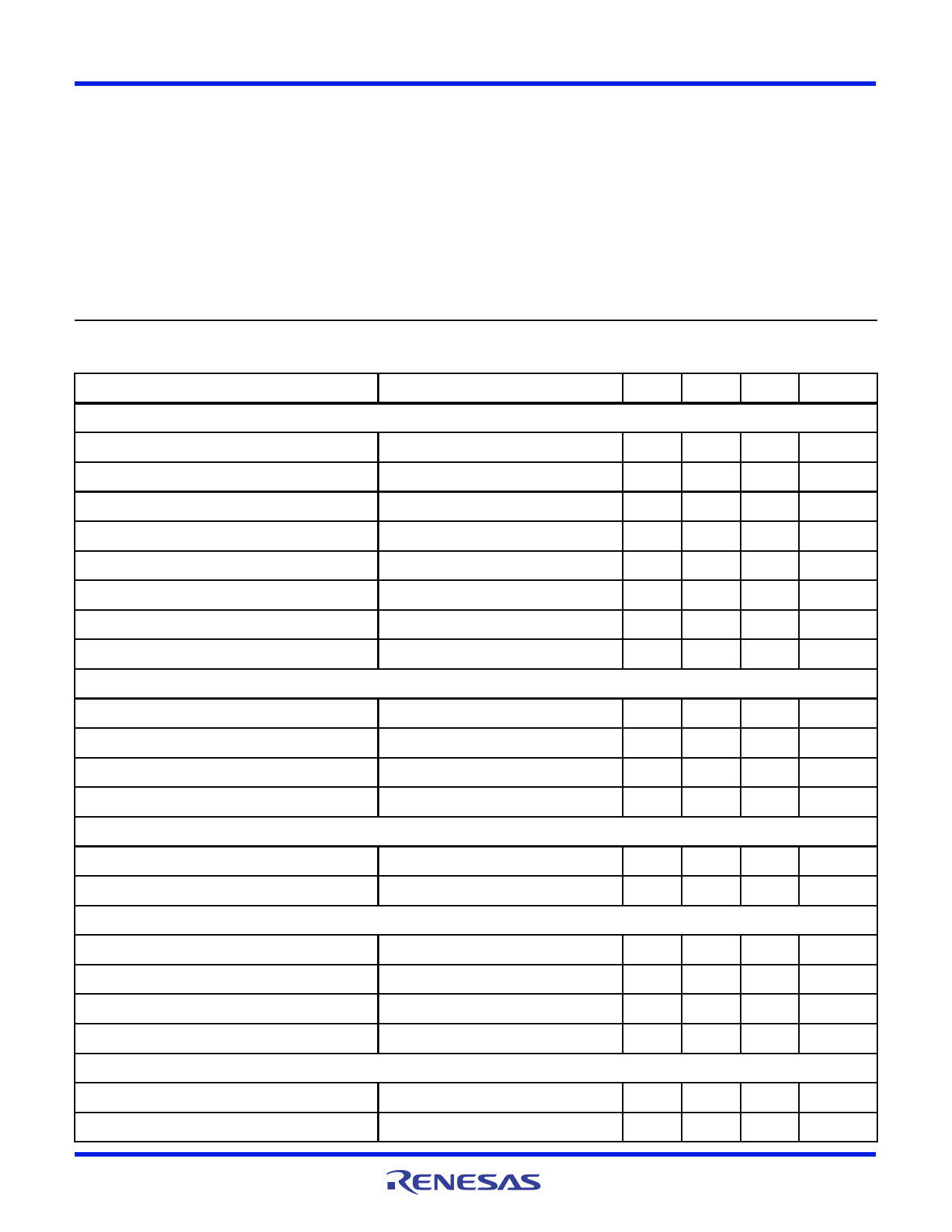
Electrical Specifications
AVDD = +4.75V to +5.25V,
CLK Pulse Width = 12.5ns,
DTVAD=D2=5o+C4.(7N5ottoe
+5.25V,
4)
VREF
=
+2.0V,
fS
=
40MHz,
PARAMETER
TEST CONDITIONS
MIN
TYP
SYSTEM PERFORMANCE
MAX
UNITS
Resolution, n
-
8
-
Bits
Integral Linearity Error, INL
Differential Linearity Error, DNL
Offset Error, VOS
Full Scale Error, FSE (Adjustable to Zero)
fS = 40MHz (End Point)
fS = 40MHz
(Note 2)
(Note 2)
-0.5
-
1.3
LSB
-
-
0.25
LSB
-
-
1
mV
-
-
13
LSB
Full Scale Output Current, IFS
Full Scale Output Voltage, VFS
Output Voltage Range, VFSR
DYNAMIC CHARACTERISTICS
-
10
15
mA
1.9
2.0
2.1
V
0.5
2.0
2.1
V
Throughput Rate
See Figure 7
40.0
-
-
MHz
Glitch Energy, GE
Differential Gain, AV (Note 3)
Differential Phase, (Note 3)
REFERENCE INPUT
ROUT = 75
-
30
-
pV-s
-
1.2
-
%
-
0.5
-
Degree
Voltage Reference Input Range
0.5
-
2.0
V
Reference Input Resistance
DIGITAL INPUTS
(Note 3)
1.0
-
-
M
Input Logic High Voltage, VIH
Input Logic Low Voltage, VIL
Input Logic Current, IIL, IIH
Digital Input Capacitance, CIN
TIMING CHARACTERISTICS
(Note 3)
(Note 3)
(Note 3)
(Note 3)
3.0
-
-
V
-
-
1.5
V
-
-
5.0
A
-
5.0
-
pF
Data Setup Time, tSU
Data Hold Time, tHLD
See Figure 1
See Figure 1
5
-
-
ns
10
-
-
ns
FN3662 Rev.3.00
October 26, 2005
Page 3 of 7
Share Link: 