HI1175 데이터 시트보기 (PDF) - Renesas Electronics
부품명
상세내역
제조사
HI1175 Datasheet PDF : 13 Pages
| |||
HI1175
Detailed Description
The HI1175 is a 2-step A/D converter featuring a 4-bit upper
comparator group and two lower comparator groups of 4 bits
each. The reference voltage can be obtained from the onboard
bias generator or be supplied externally. This IC uses an offset
canceling type comparator that operates synchronously with an
external clock. The operating modes of the part are input
sampling (S), hold (H), and compare (C).
The operation of the part is illustrated in Figure 2. A reference
voltage that is between VRT-VRB is constantly applied to the
upper 4-bit comparator group. VI(1) is sampled with the falling
edge of the first clock by the upper comparator block. The
lower block A also samples VI(1) on the same edge. The upper
comparator block finalizes comparison data MD(1) with the
rising edge of the first clock. Simultaneously the reference
supply generates a reference voltage RV(1) that corresponds
to the upper results and applies it to the lower comparator
block A. The lower comparator block finalizes comparison data
LD(1) with the rising edge of the second clock. MD(1) and
LD(1) are combined and output as OUT(1) with the rising edge
of the third clock. There is a 2.5 cycle clock delay from the
analog input sampling point to the corresponding digital output
data. Notice how the lower comparator blocks A and B
alternate generating the lower data in order to increase the
overall A/D sampling rate.
Test Circuits
+V
Power, Grounding, and Decoupling
To reduce noise effects, separate the analog and digital
grounds.
In order to avoid latchup at power up, it is necessary that AVDD
and DVDD be driven from the same supply.
Bypass both the digital and analog VDD pins to their respective
grounds with a ceramic 0.1F capacitor close to the pin.
Analog Input
The input capacitance is small when compared with other flash
type A/D converters. However, it is necessary to drive the input
with an amplifier with sufficient bandwidth and drive capability.
In order to prevent parasitic oscillation, it may be necessary to
insert a low value (i.e., 0.24) resistor between the output of
the amplifier and the A/D input.
Reference Input
The range of the A/D is set by the voltage between VRT and
VRB. The internal bias generator will set VRTS to 2.6V and
VRBS to 0.6V. These can be used as the part reference by
shorting VRT and VRTS and VRB to VRBS. The analog input
range of the A/D will now be from 0.6V to 2.6V and is referred
to as Self Bias Mode 1. Self Bias Mode 2 is where VRB is
connected to AGND and VRT is shorted to VRTS. The analog
input range will now be from 0V to 2.4V.
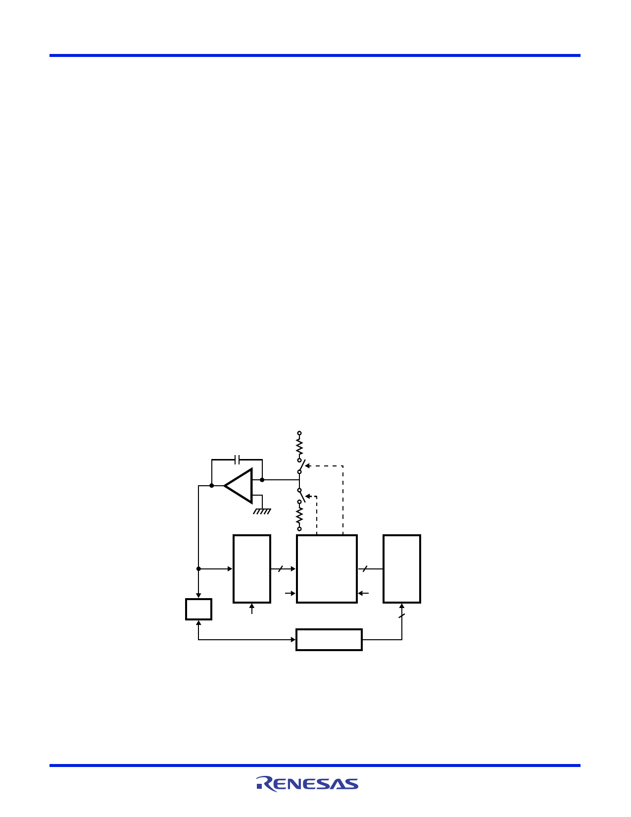
S2
-
S1 : ON IF A < B
+
S1
S2 : ON IF A > B
-V
A<B A>B
VIN
DUT
HI1175
DVM
COMPARATOR
8
A8
B8
8
TO
TO
A1
B1
“0” A0
B0 “1”
CLK (20MHz)
CONTROLLER
BUFFER
000 • • • 00
8
TO
111 • • • 10
FIGURE 21. INTEGRAL AND DIFFERENTIAL NON-LINEARITY ERROR AND OFFSET VOLTAGE TEST CIRCUIT
FN3577 Rev 8.00
October 25, 2005
Page 10 of 13
Share Link: 