LC72140M 데이터 시트보기 (PDF) - SANYO -> Panasonic
부품명
상세내역
제조사
LC72140M Datasheet PDF : 15 Pages
| |||
LC72140, 72140M
Continued from preceding page.
Name
Function
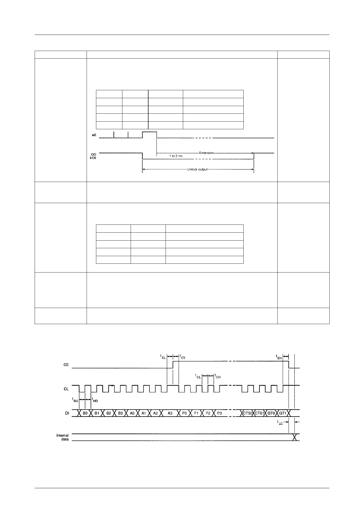
PLL unlock detect control
Bits UL0 UL1 select the phase error threshold and extension (φE) used to detect the PLL
unlocked state as shown in Table 10 and Figure 4. When the phase error is greater than the
selected error, the PLL unlock detector output goes LOW.
UL0, UL1
Table 10. Unlock detection and extension selection
UL1
UL0
Phase error
Detector output
0
0
Stopped
Open
0
1
0
φE output
1
0
±0.56µs
φE with 1 to 2ms extension
1
1
±1.11µs
φE with 1 to 2ms extension
Related bits
ULD, DT0, DT1
XS
DZ0, DZ1
DLC
TEST0 to TEST2
Figure 4. Phase-error extension
Crystal oscillator control
Bit XS selects the oscillator frequency. When XS is 1, the frequency is 7.2MHz, and when XS is 0,
4.5MHz.
4.5MHz is selected after power-ON reset.
Phase comparator control
Bits DZ0 and DZ1 select the phase comparator insensitive band, or dead zone.
Table 11. Insensitive band mode selection
DZ1
DZ0
Insensitive band (dead zone) mode
0
0
DZA
0
1
DZB
1
0
DZC
1
1
DZD
DZA is selected after power-ON reset.
Charge pump control
Bit DLC controls the charge pump operation. When DLC is 1, the charge pump outputs are forced
to LOW, and when DLC is 0, the charge pump operates normally.
This feature can be useful to remove the PLL from a deadlock state. The PLL can deadlock if its
VCO control voltage Vtune becomes 0V, halting the VCO. Setting DLC to 1 sets Vtune to VCC,
restarting the VCO.
Normally operating mode is selected after power-ON reset.
Test data
Bits TEST0 to TEST2 are used for in-factory device testing. Set them all to 0. They are set to zero
after a power-ON reset.
Serial Data Input Timing
The timing for the serial data input words is shown in Figure 5. The first eight bits are the mode select bits.
Figure 5. Input timing
Notes
1. tSU, tHD, tEL, tES, tCL, tCH and tEH>0.45µs
2. tLC<0.45µs
No.4464–9/15
Share Link: 