NJU6631ACH 데이터 시트보기 (PDF) - Japan Radio Corporation
부품명
상세내역
제조사
NJU6631ACH Datasheet PDF : 32 Pages
| |||
NJU6631A
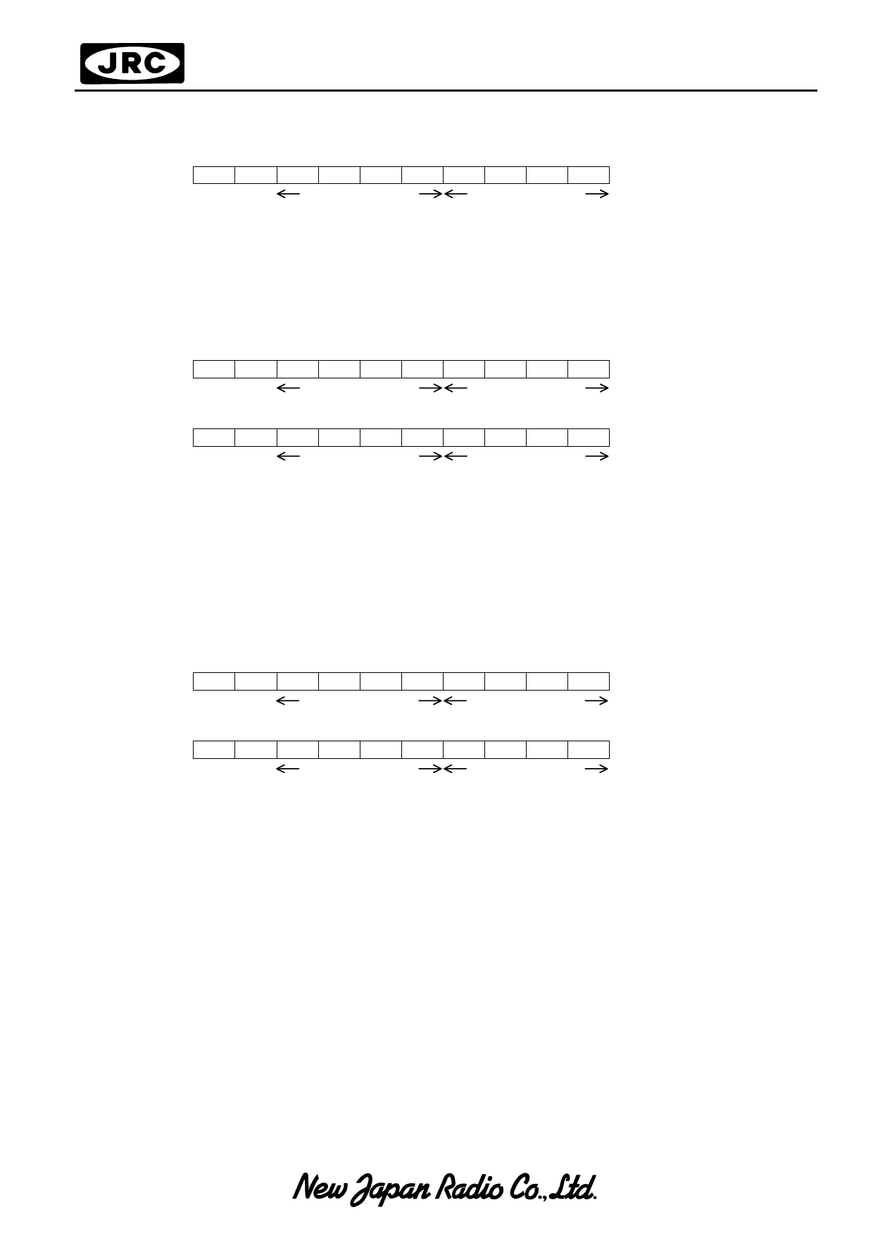
(j) Read Busy Flag & Address
RS R/W DB7 DB6 DB5 DB4 DB3 DB2 DB1 DB0
Code 0 1 BF A A A A A A A
Higher order bit
Lower order bit
This instruction reads out the internal status of the NJU6631A. When this instruction is executed, the busy
flag (BF) which indicate internal operation is read out from DB7 and the address of CG RAM or DD RAM is
read out from DB6 to DB0 (the address for CG RAM or DD RAM is determined by the previous instruction).
(BF)=1 indicates that internal operation is in progress. The next instruction is inhibited when (BF)=1.
Check the (BF) status before the next write operation.
(k) Write Data to CG or DD RAM
RS R/W DB7 DB6 DB5 DB4 DB3 DB2 DB1 DB0
Code 1 0 D D D D D D D D (DD RAM)
Higher order bit
Lower order bit
RS R/W DB7 DB6 DB5 DB4 DB3 DB2 DB1 DB0
Code 1 0 * * * D D D D D (CG RAM)
Higher order bit
Lower order bit
Write Data to CG RAM or DD RAM instruction is executed when the code "1" is written into (RS) and code
"0" is written into (R/W).
By the execution of this instruction, the binary 5-bit data "DDDDD" are written into the CG RAM, and the
binary 8-bit data "DDDDDDDD" are written into the DD RAM. The selection of the CG RAM or DD RAM is
determined by the previous instruction.
After this instruction execution, the address increment (+1) or decrement (-1) performed automatically
according to the entry mode set. And the display shift is also executed according to the previous entry mode
set.
(l) Read Data from CG or DD RAM
RS R/W DB7 DB6 DB5 DB4 DB3 DB2 DB1 DB0
Code 1 1 D D D D D D D D (DD RAM)
Higher order bit
Lower order bit
RS R/W DB7 DB6 DB5 DB4 DB3 DB2 DB1 DB0
Code 1 1 * * * D D D D D (CG RAM)
Higher order bit
Lower order bit
Read Data from CG RAM or DD RAM instruction is executed when the code "1" is written into (RS) and
(R/W).
By the execution of this instruction, the binary 5 bit data "DDDDD" are read out from CG RAM, and the
binary 8 bit data "DDDDDDDD" are read out from DD RAM. The selection of the CG RAM or DD RAM is
determined by the previous instruction.
Before executing this instruction, either the CG RAM address set or DD RAM address set must be executed,
otherwise the first read out data are invalidated.
When this instruction is serially executed, the next address data is normally read from the second read.
The address set instruction is not required if the cursor shift instruction is executed just beforehand (only DD
RAM reading).
The cursor shift instruction has same function as the DD RAM address set, so that after reading the DD
RAM, the address increment or decrement is executed automatically according to the entry mode.
But display shift does not occur regardless of the entry mode.
Note : The address counter(AC) is automatically incremented or decremented by 1 after write instructions to
either of the CG RAM or DD RAM. Even if the read instruction is executed after this instruction, the
addressed data can not be read out correctly. For a correct data read out, either the address set
instruction or cursor shift instruction (only with DD RAM) must be implemented just before this
instruction or from the second time read out instruction execution if the read out instruction is
executed 2 times consecutively.
Share Link: 