ADP122 데이터 시트보기 (PDF) - Analog Devices
부품명
상세내역
제조사
ADP122 Datasheet PDF : 24 Pages
| |||
Data Sheet
5.5 V Input, 300 mA, Low Quiescent
Current, CMOS Linear Regulator
ADP122/ADP123
FEATURES
Input voltage supply range: 2.3 V to 5.5 V
300 mA maximum output current
Fixed and adjustable output voltage versions
Very low dropout voltage: 85 mV at 300 mA load
Low quiescent current: 45 µA at no load
Low shutdown current: <1 µA
Initial accuracy: ±1% accuracy
Up to 31 fixed-output voltage options available from
1.75 V to 3.3 V
Adjustable-output voltage range
0.8 V to 5.0 V (ADP123)
Excellent PSRR performance: 60 dB at 100 kHz
Excellent load/line transient response
Optimized for small 1.0 μF ceramic capacitors
Current limit and thermal overload protection
Logic controlled enable
Compact packages: 5-lead TSOT and 6-lead 2 mm × 2 mm LFCSP
APPLICATIONS
Digital camera and audio devices
Portable and battery-powered equipment
Automatic meter reading (AMR) meters
GPS and location management units
Medical instrumentation
Point-of-sale equipment
GENERAL DESCRIPTION
The ADP122/ADP123 are low quiescent current, low dropout
linear regulators. They are designed to operate from an input
voltage between 2.3 V and 5.5 V and to provide up to 300 mA of
output current. The low 85 mV dropout voltage at a 300 mA load
improves efficiency and allows operation over a wide input
voltage range.
The low 170 μA of quiescent current at full load makes the ADP122
ideal for battery-operated portable equipment.
The ADP122 is capable of 31 fixed output voltages from 1.75 V
to 3.3 V. The ADP123 is the adjustable version of the device and
allows the output voltage to be set between 0.8 V and 5.0 V by
an external voltage divider.
The ADP122/ADP123 are specifically designed for stable operation
with tiny 1 µF ceramic input and output capacitors to meet the
requirements of high performance, space constrained applications.
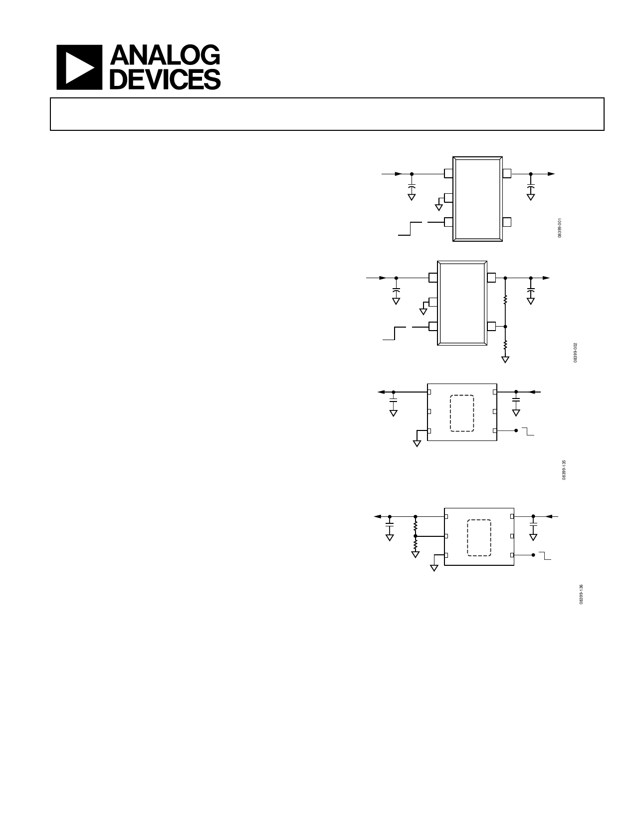
TYPICAL APPLICATION CIRCUITS
VIN = 2.3V TO 5.5V
CIN
1µF
1 VIN VOUT 5
ADP122
2 GND
VOUT = 1.8V
COUT
1µF
ON
OFF
3 EN
NC 4
Figure 1. ADP122 with Fixed Output Voltage (TSOT Version)
VIN = 2.3V TO 5.5V
CIN
1µF
1 VIN VOUT 5
ADP123
2 GND
VOUT = 0.5V(1 + R1/R2)
COUT
1µF
R1
ON
OFF
3 EN
ADJ 4
R2
Figure 2. ADP123 with Adjustable Output Voltage (TSOT Version)
VOUT = 1.8V 1
C2
1µF
GND 2
VOUT
NC
3
GND
6 VIN = 2.3V TO 5.5V
VIN
C1
1µF
NC 5
GND
4
EN
ON
OFF
GND
ADP122
TOP VIEW
(Not to Scale)
NC = NOT CONNECT. THIS PIN CAN BE LEFT FLOATING
OR CONNECTED TO GROUND.
Figure 3. ADP122 with Fixed Output Voltage (LFCSP Version)
VOUT = 0.5V (1 + R1/R2) 1
C2
1µF
R1
2
GND
R2
3
GND
VOUT
ADJ
GND
6 VIN = 2.3V TO 5.5V
VIN
C1
1µF
NC 5
GND
4
EN
ON
OFF
GND
ADP123
TOP VIEW
(Not to Scale)
NC = NOT CONNECT. THIS PIN CAN BE LEFT FLOATING
OR CONNECTED TO GROUND.
Figure 4. ADP123 with Adjustable Output Voltage (LFCSP Version)
The ADP122/ADP123 have an internal soft start that gives a
constant start-up time of 350 µs. Short-circuit protection and
thermal overload protection circuits prevent damage in adverse
conditions. The ADP122/ADP123 are available in a tiny, 5-lead
TSOT package and 6-lead LFCSP package for the smallest
footprint solution to meet a variety of portable applications.
Rev. E
Information furnished by Analog Devices is believed to be accurate and reliable. However, no
responsibility is assumed by Analog Devices for its use, nor for any infringements of patents or other
rights of third parties that may result from its use. Specifications subject to change without notice. No
license is granted by implication or otherwise under any patent or patent rights of Analog Devices.
Trademarks and registered trademarks are the property of their respective owners.
One Technology Way, P.O. Box 9106, Norwood, MA 02062-9106, U.S.A.
Tel: 781.329.4700
www.analog.com
Fax: 781.461.3113 ©2009–2012 Analog Devices, Inc. All rights reserved.
Share Link: 