LC75810E 데이터 시트보기 (PDF) - ON Semiconductor
부품명
상세내역
제조사
LC75810E Datasheet PDF : 54 Pages
| |||
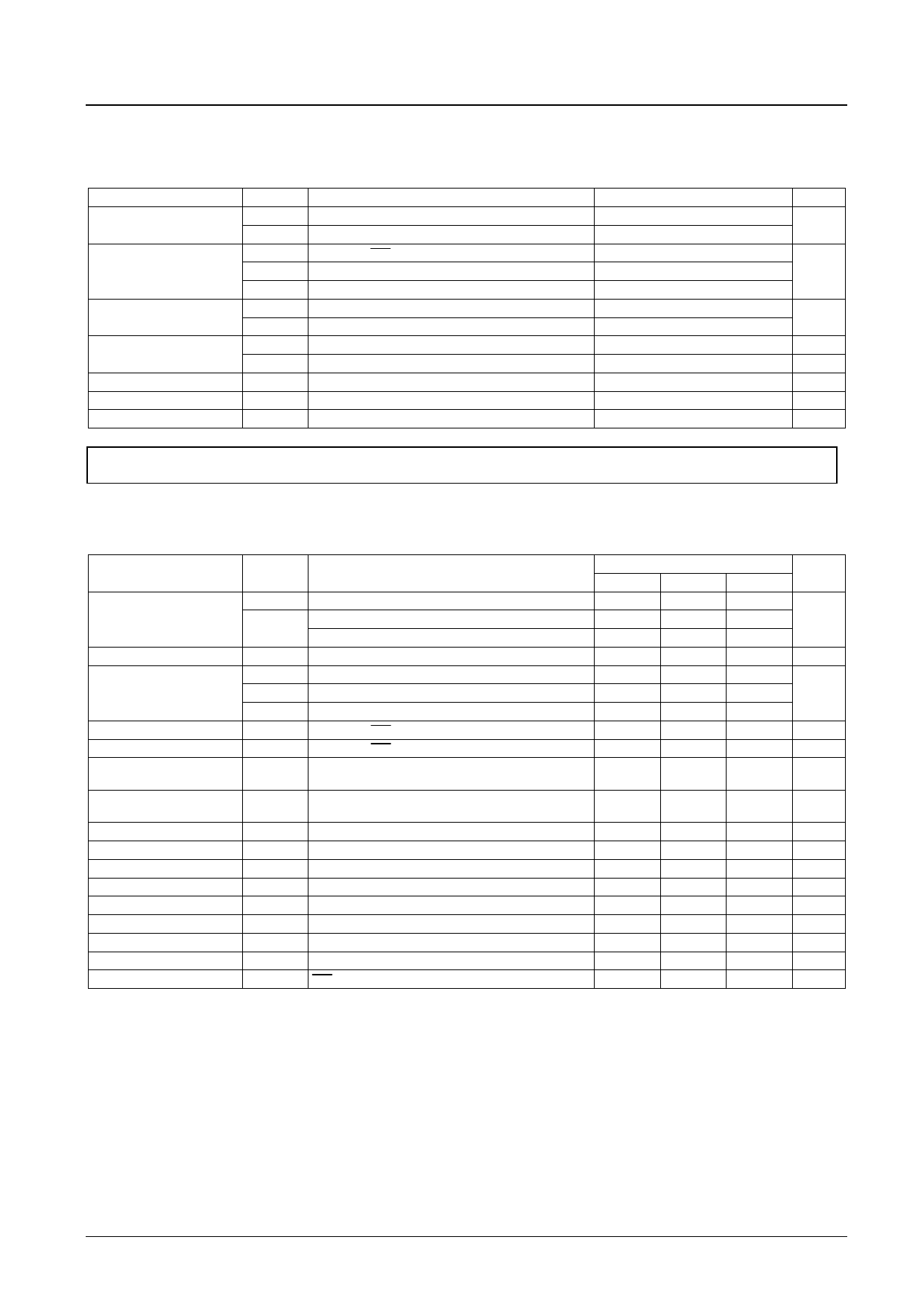
Specifications
LC75810E/T
Absolute Maximum Ratings at Ta = 25°C, VSS = 0V
Parameter
Maximum supply voltage
Input voltage
Output voltage
Output current
Allowable power dissipation
Operating temperature
Storage temperature
Symbol
VDD max
VLCD max
VIN1
VIN2
VIN3
VOUT1
VOUT2
IOUT1
IOUT2
Pd max
Topr
Tstg
Conditions
VDD
VLCD
CE, CL, DI, RES
OSC
VLCD1, VLCD2, VLCD3
OSC
VLCD0, S1 to S80, COM1 to COM10
S1 to S80
COM1 to COM10
Ta = 85°C
Ratings
Unit
−0.3 to +7.0
V
−0.3 to +11.0
−0.3 to +7.0
−0.3 to VDD + 0.3
V
−0.3 to VLCD + 0.3
−0.3 to VDD+ 0.3
V
−0.3 to VLCD + 0.3
300
μA
3 mA
200 mW
−40 to +85
°C
−55 to +125
°C
Stresses exceeding Maximum Ratings may damage the device. Maximum Ratings are stress ratings only. Functional operation above the Recommended Operating
Conditions is not implied. Extended exposure to stresses above the Recommended Operating Conditions may affect device reliability.
Allowable Operating Ranges at Ta = −40°C to + 85°C, VSS = 0V
Parameter
Supply voltage
Output voltage
Input voltage
Input high level voltage
Input low level voltage
Recommended external
resistance
Recommended external
capacitance
Guaranteed oscillation range
Data setup time
Data hold time
CE wait time
CE setup time
CE hold time
High level clock pulse width
Low level clock pulse width
Minimum reset pulse width
Symbol
Conditions
VDD
VLCD
VLCD0
VLCD1
VLCD2
VLCD3
VIH
VIL
Rosc
VDD
When the display contrast adjustment circuit is used.
When the display contrast adjustment circuit is not used.
VLCD0
VLCD1
VLCD2
VLCD3
CE, CL, DI, RES
CE, CL, DI, RES
OSC
Cosc
fosc
tds
tdh
tcp
tcs
tch
tφH
tφL
tWRES
OSC
OSC
CL, DI
CL, DI
CE, CL
CE, CL
CE, CL
CL
CL
RES
(Figure 2)
(Figure 2)
(Figure 2)
(Figure 2)
(Figure 2)
(Figure 2)
(Figure 2)
(Figure 3)
min.
2.7
7.0
4.5
4.5
0.8 VDD
0
Ratings
typ.
3/4 VLCD0
2/4 VLCD0
1/4 VLCD0
10
470
150
300
160
160
160
160
160
160
160
1
Unit
max.
6.0
10.0
V
10.0
VLCD
V
VLCD0
VLCD0
V
VLCD0
6.0
V
0.2 VDD
V
kΩ
pF
600 kHz
ns
ns
ns
ns
ns
ns
ns
μs
No.7141-4/54
Share Link: 