LTC1142 데이터 시트보기 (PDF) - Linear Technology
부품명
상세내역
제조사
LTC1142 Datasheet PDF : 20 Pages
| |||
LTC1142/LTC1142L/LTC1142HV
W
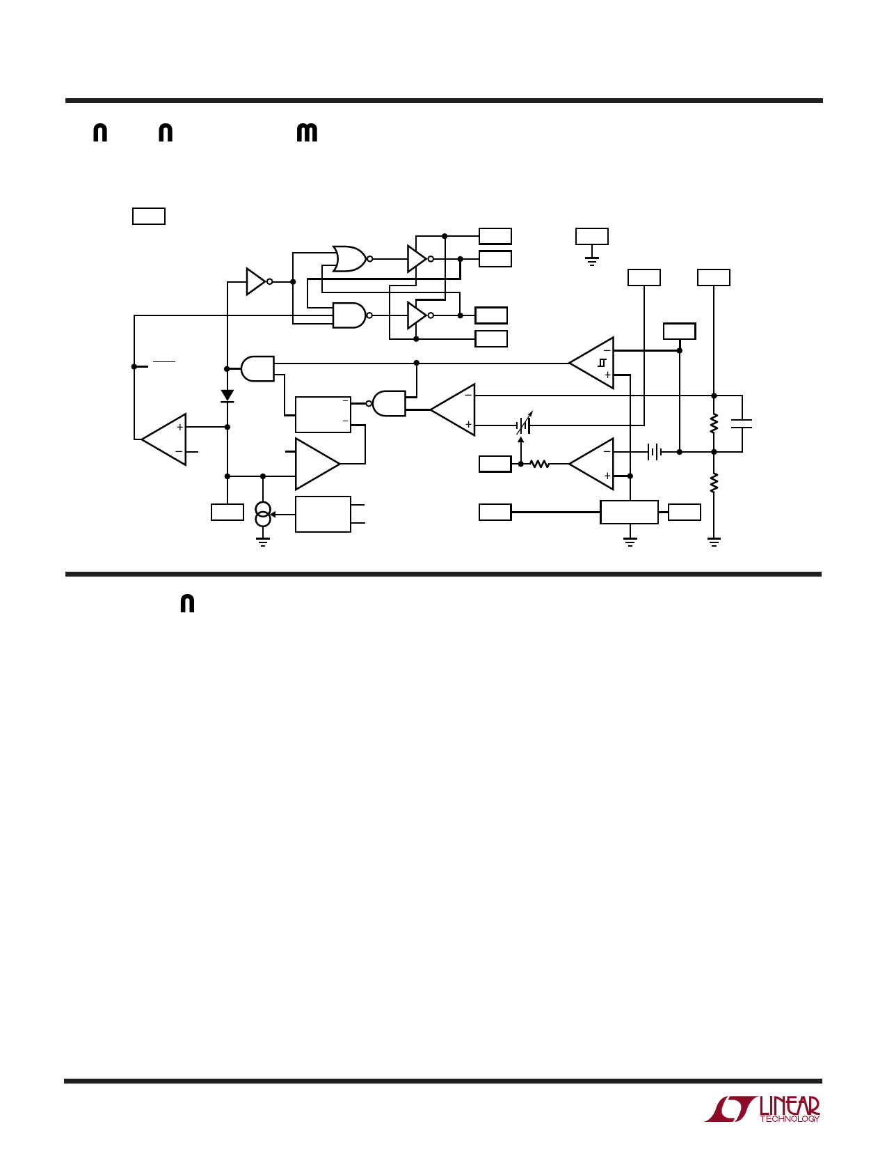
FU CTIO AL DIAGRA
Only one regulator block shown. Pin numbers are for 3.3V (5V) sections for LTC1142/LTC1142HV,
and VOUT1 (VOUT2) for LTC1142L-ADJ/LTC1142HV-ADJ.
2(16)
LTC1142-ADJ
3(17)
PIN NUMBERS FOR
LTC1142, LTC1142HV
PIN NUMBERS
FOR LTC1142L-ADJ
LTC1142HV-ADJ
SLEEP
24(10) VIN
23(9) PDRIVE
6(20) NDRIVE
4(18) PGND
LTC1142L-ADJ, LTC1142HV-ADJ: 5(19)
SGND
3(17)
LTC1142L-ADJ
LTC1142HV-ADJ
4(18)
SENSE+
SENSE–
1(15)
28(14)
LTC1142L-ADJ
LTC1142HV-ADJ
2(16)
NC/ADJ
V
S
VTH2
R
Q
S
VTH1 –
T
+
25(11)
CT
OFF-TIME
CONTROL
VIN
SENSE–
C
25mV TO 150mV
–+
ITH
13k
27(13)
SHDN
2(16)
LTC1142L-ADJ
LTC1142HV-ADJ
3(17)
VOS
G
1.25V
REFERENCE
INTVCC
26(12)
5pF
100k
1142 BD
U
OPERATIO Refer to Functional Diagram
The LTC1142 series consists of two individual regulator
blocks, each using current mode, constant off-time archi-
tectures to synchronously switch an external pair of
complementary power MOSFETs. The two regulators are
internally set to provide output voltages of 3.3V and 5V for
the LTC1142. The LTC1142HV-ADJ/LTC1142L-ADJ are
configured to provide two user selectable output voltages,
each set by external resistor dividers. Operating fre-
quency is individually set on each section by the external
capacitors at CT, Pins 11 and 25.
The output voltage is sensed by an internal voltage divider
connected to Sense –, Pin 28 (14) (LTC1142) or external
divider returned to VFB, Pin 2 (16) (LTC1142-ADJ). A
voltage comparator V and a gain block G compare the
divided output voltage with a reference voltage of 1.25V.
To optimize efficiency, the LTC1142 series automatically
switches between two modes of operation, Burst Mode
and continuous mode. The voltage comparator is the
primary control element when the device is in Burst Mode
operation, while the gain block controls the output voltage
in continuous mode.
During the switch “ON” cycle in continuous mode, current
comparator C monitors the voltage between Pins 1 (15)
and 28 (14) connected across an external shunt in series
with the inductor. When the voltage across the shunt
reaches its threshold value, the PDrive output is switched
to VIN, turning off the P-channel MOSFET. The timing
capacitor connected to Pin 25 (11) is now allowed to
discharge at a rate determined by the off-time controller.
The discharge current is made proportional to the output
voltage [measured by Pin 28 (14)] to model the inductor
current, which decays at a rate that is also proportional to
the output voltage. While the timing capacitor is discharg-
ing, the NDrive output goes to VIN, turning on the N-channel
MOSFET.
When the voltage on the timing capacitor has discharged
past VTH1, comparator T trips, setting the flip-flop. This
causes the NDrive output to go low (turning off the
N-channel MOSFET) and the PDrive output to also go low
(turning the P-channel MOSFET back on). The cycle then
repeats.
8
Share Link: 