CXD1171 데이터 시트보기 (PDF) - Harris Semiconductor
부품명
상세내역
제조사
CXD1171 Datasheet PDF : 8 Pages
| |||
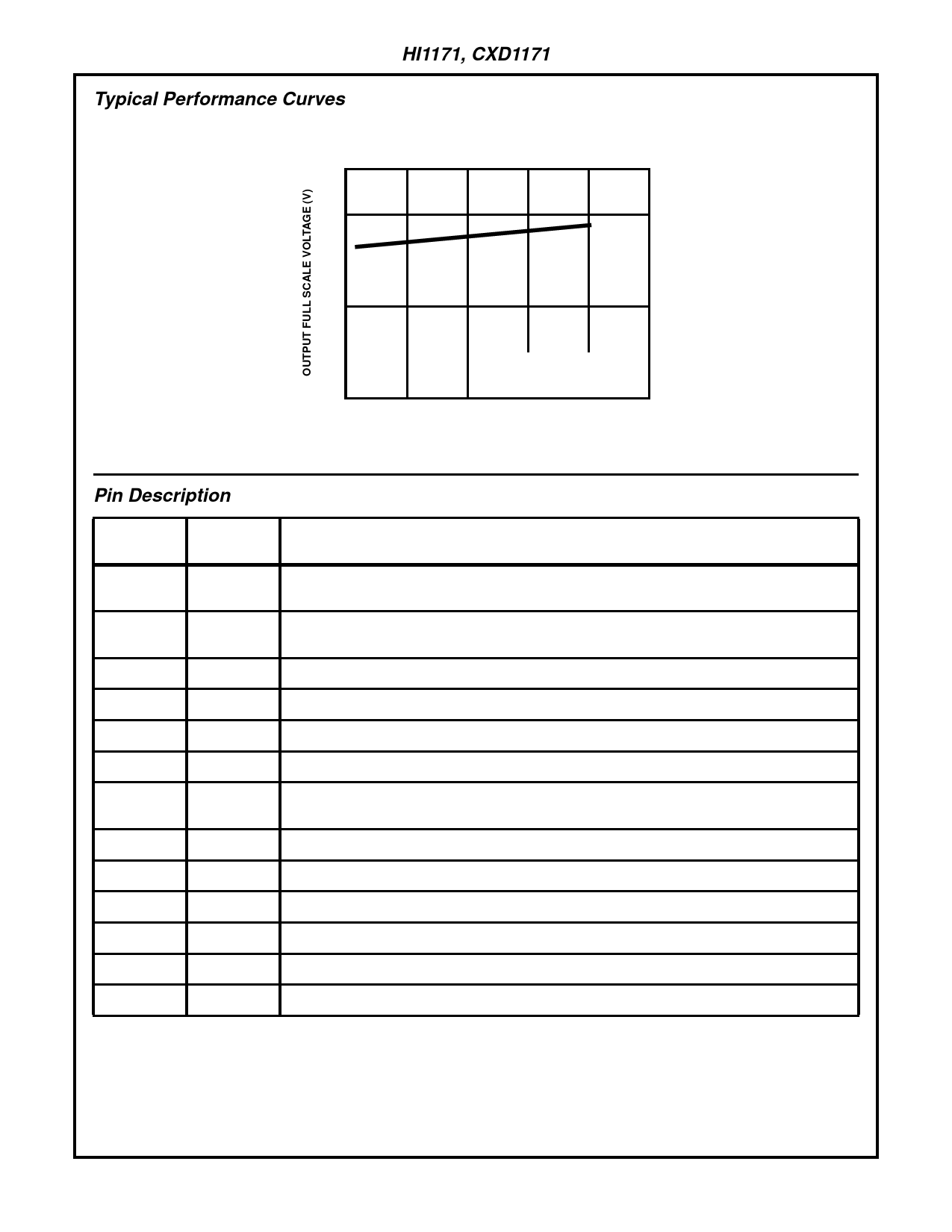
Typical Performance Curves
HI1171, CXD1171
2.0
1.9
VDD = 5.0V, VREF = 2.0V
R = 200Ω, 16R = 3.3kΩ
TA = +25oC
0
-25
0
25
50
75
AMBIENT TEMPERATURE (oC)
FIGURE 6. OUTPUT FULL SCALE VOLTAGE vs AMBIENT TEMPERATURE
Pin Description
24 PIN
SOIC
1-8
9
10, 13
11
12
14
15
16
17
18, 19, 22
20
21
23, 24
PIN
NAME
PIN DESCRIPTION
D0(LSB) thru Digital Data Bit 0, the Least Significant Bit thru Digital Data Bit 7, the Most Significant Bit
D7(MSB)
BLNK
Blanking Line, used to clear the internal data register to the zero condition when High, normal operation
when Low.
DVSS
VB
CLK
Digital Ground
Voltage Bias, connect a 0.1µF capacitor to DVSS
Data Clock Pin 100kHz to 40MHz
AVSS
IREF
VREF
VG
AVDD
IOUT1
IOUT2
DVDD
Analog Ground
Current Reference, used to set the current range. Connect a resistor to AVSS that is 16 times greater
than the resistor on IOUT1. (See Typical Applications Circuit)
Input Reference Voltage used to set the output full scale range.
Voltage Ground, connect a 0.1µF capacitor to AVDD.
Analog Supply 4.75V to 7V
Current Output Pin.
Current Output pin used for a virtual ground connection. Usually connected to AVSS
Digital Supply 4.75V to 7V
5
Share Link: 