MC100LVEL11DG 데이터 시트보기 (PDF) - ON Semiconductor
부품명
상세내역
제조사
MC100LVEL11DG Datasheet PDF : 8 Pages
| |||
MC100LVEL11
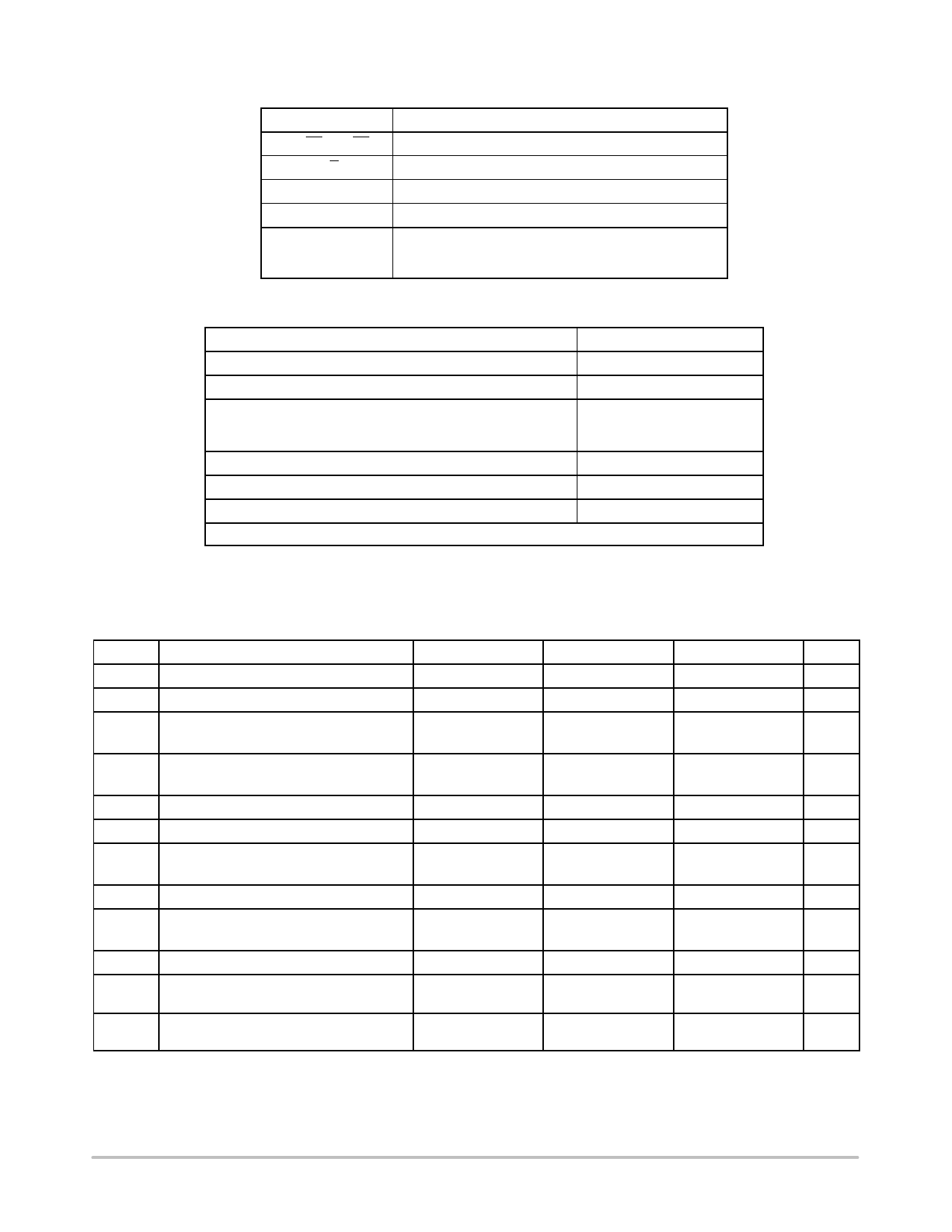
Table 1. PIN DESCRIPTION
Pin
ÁÁÁÁÁÁÁÁÁÁÁÁÁÁÁÁÁÁÁÁÁ Q0, Q0; Q1, Q1
ÁÁÁÁÁÁÁÁÁÁÁÁÁÁÁÁÁÁÁÁÁ D, D
ÁÁÁÁÁÁÁÁÁÁÁÁÁÁÁÁÁÁÁÁÁ VCC
ÁÁÁÁÁÁÁÁÁÁÁÁÁÁÁÁÁÁÁÁÁ VEE
ÁÁÁÁÁÁÁÁÁÁÁÁÁÁÁÁÁÁÁÁÁÁÁÁÁÁÁÁÁÁÁÁÁÁÁÁÁÁÁÁÁÁÁÁÁÁÁÁÁÁÁÁÁÁÁÁÁÁÁÁÁÁÁ EP
Function
ECL Data Outputs
ECL Data Inputs
Positive Supply
Negative Supply
Exposed pad must be connected to a sufficient thermal
conduit. Electrically connect to the most negative supply
or leave floating open.
Table 2. ATTRIBUTES
Characteristics
Internal Input Pulldown Resistor
Internal Input Pullup Resistor
ESD Protection
Human Body Model
Machine Model
Charge Device Model
Moisture Sensitivity, Indefinite Time Out of Drypack (Note 1)
Flammability Rating
Oxygen Index: 28 to 34
Transistor Count
Meets or exceeds JEDEC Spec EIA/JESD78 IC Latchup Test
1. For additional information, see Application Note AND8003/D.
Value
75 kW
75 kW
> 4 KV
> 400 V
> 2 kV
Level 1
UL 94 V−0 @ 0.125 in
63
Table 3. MAXIMUM RATINGS
Symbol
VCC
VEE
VI
Iout
TA
Tstg
qJA
qJC
qJA
qJC
qJA
Parameter
PECL Mode Power Supply
NECL Mode Power Supply
PECL Mode Input Voltage
NECL Mode Input Voltage
Output Current
Operating Temperature Range
Storage Temperature Range
Thermal Resistance (Junction−to−Ambient)
Thermal Resistance (Junction−to−Case)
Thermal Resistance (Junction−to−Ambient)
Thermal Resistance (Junction−to−Case)
Thermal Resistance (Junction−to−Ambient)
Condition 1
VEE = 0 V
VCC = 0 V
VEE = 0 V
VCC = 0 V
Continuous
Surge
0 lpfm
500 lpfm
Standard Board
0 lpfm
500 lpfm
Standard Board
0 lfpm
500 lfpm
Condition 2
VI VCC
VI VEE
SOIC−8
SOIC−8
SOIC−8
TSSOP−8
TSSOP−8
TSSOP−8
DFN8
DFN8
Rating
8 to 0
−8 to 0
6 to 0
−6 to 0
50
100
−40 to +85
−65 to +150
190
130
41 to 44 ± 5%
185
140
41 to 44 ± 5%
129
84
Units
V
V
V
mA
mA
°C
°C
°C/W
°C/W
°C/W
°C/W
°C/W
°C/W
°C/W
°C/W
Tsol
Wave Solder
Pb <2 to 3 sec @ 248°C
Pb−Free <2 to 3 sec @ 260°C
265
°C
265
Stresses exceeding Maximum Ratings may damage the device. Maximum Ratings are stress ratings only. Functional operation above the
Recommended Operating Conditions is not implied. Extended exposure to stresses above the Recommended Operating Conditions may affect
device reliability.
http://onsemi.com
2
Share Link: 