AZ100LVEL16 데이터 시트보기 (PDF) - AZ Microtek
부품명
상세내역
제조사
AZ100LVEL16 Datasheet PDF : 7 Pages
| |||
AZ10LVEL16 ARIZONA MICROTEK, INC.
AZ100LVEL16
ECL/PECL Differential Receiver
FEATURES
PACKAGE AVAILABILITY
• Green and RoHS Compliant / Lead (Pb)
Free Packages available
• 250ps Propagation Delay
• High Bandwidth Output Transitions
• Operating Range of 3.0V to 5.5V
• Internal Input Pulldown Resistors
• Direct Replacement For ON
PACKAGE
SOIC 8
SOIC 8
SOIC 8 RoHS
Compliant / Lead
(Pb) Free
PART NUMBER
AZ10LVEL16D
AZ100LVEL16D
MARKING
AZM10
LVEL16
AZM100
LVEL16
AZ100LVEL16D+
AZM100+
LVEL16
NOTES
1,2
1,2
1,2
Semiconductor MC10EL16, MC100EL16,
& MC100LVEL16
TSSOP 8
AZ10LVEL16T
AZT
LV16
1,2
• IBIS Model Files Available on Arizona
Microtek Website
TSSOP 8 RoHS
Compliant / Lead
(Pb) Free
AZ10LVEL16T+
AZT+
LV16
1,2
TSSOP 8
AZ100LVEL16T
AZH
LV16
1,2
DESCRIPTION
TSSOP 8 RoHS
Compliant / Lead
(Pb) Free
AZ100LVEL16T+
AZH+
LV16
1,2
The AZ10/100LVEL16 is a differential
receiver. The device is functionally equivalent
to the E116 device with higher performance
capabilities. With output transition times
significantly faster than the E116, the LVEL16
MLP 8 (2x2)
Green / RoHS
Compliant / Lead
AZ100LVEL16NG
Q6G
<Date Code>
1,3
(Pb) Free
1 Add R1 at end of part number for 7 inch (1K parts), R2 for 13 inch (2.5K parts)
Tape & Reel.
is ideally suited for interfacing with high
frequency sources.
The LVEL16 provides a VBB output for
2 Date code format: “Y” or “YY” for year followed by “WW” for week on
underside of part.
3 Date code format: “Y” for year followed by “WW” for week.
single-ended use or a DC bias reference for AC coupling to the device. For single-ended input applications, the VBB
reference should be connected to one side of the D/D¯ differential input pair. The input signal is then fed to the other
D/D¯ input. The VBB pin can support 1.5 mA sink/source current. When used, the VBB pin should be bypassed to
ground via a 0.01 μF capacitor.
Under open input conditions internal input clamps will force the Q output LOW.
NOTE: Specifications in the ECL/PECL tables are valid when thermal equilibrium is established.
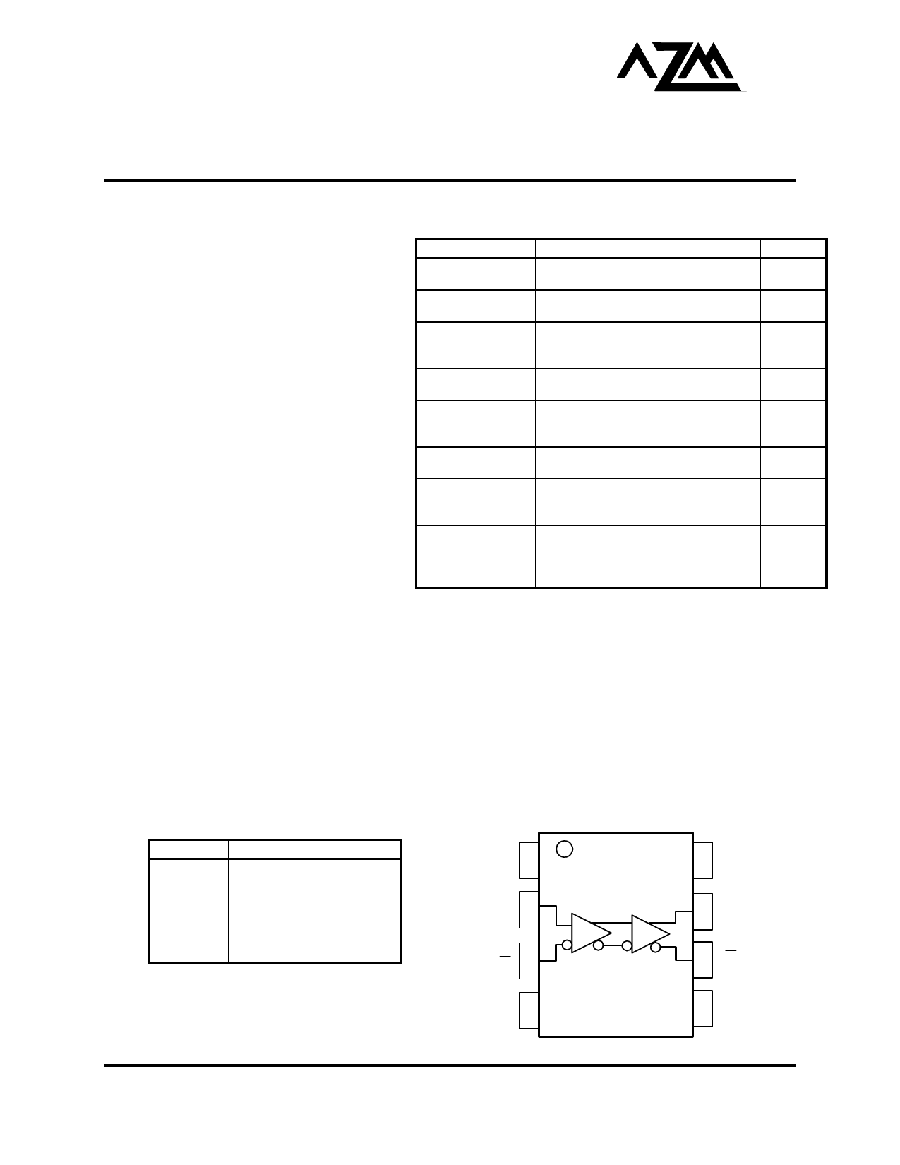
PIN DESCRIPTION
PIN
D, D¯
Q, Q¯
VBB
VCC
VEE
NC
FUNCTION
Data Inputs
Data Outputs
Reference Voltage Output
Positive Supply
Negative Supply
No Connect
PINOUT ASSIGNMENT
NC 1
D2
D3
8 VCC
7Q
6Q
VBB 4
5 VEE
1630 S. STAPLEY DR., SUITE 127 • MESA, ARIZONA 85204 • USA • (480) 962-5881 • FAX (480) 890-2541
www.azmicrotek.com
Share Link: 