LCX024AKB 데이터 시트보기 (PDF) - Sony Semiconductor
부품명
상세내역
제조사
LCX024AKB Datasheet PDF : 24 Pages
| |||
LCX024AKB
Level Conversion Circuit
The LCX024AKB has a built-in level conversion circuit in the clock input unit located inside the panel. The
circuit voltage is stepped up to VDD inside the panel. This level conversion circuit meets the specifications of a
3.0V power supply of the externally-driven IC.
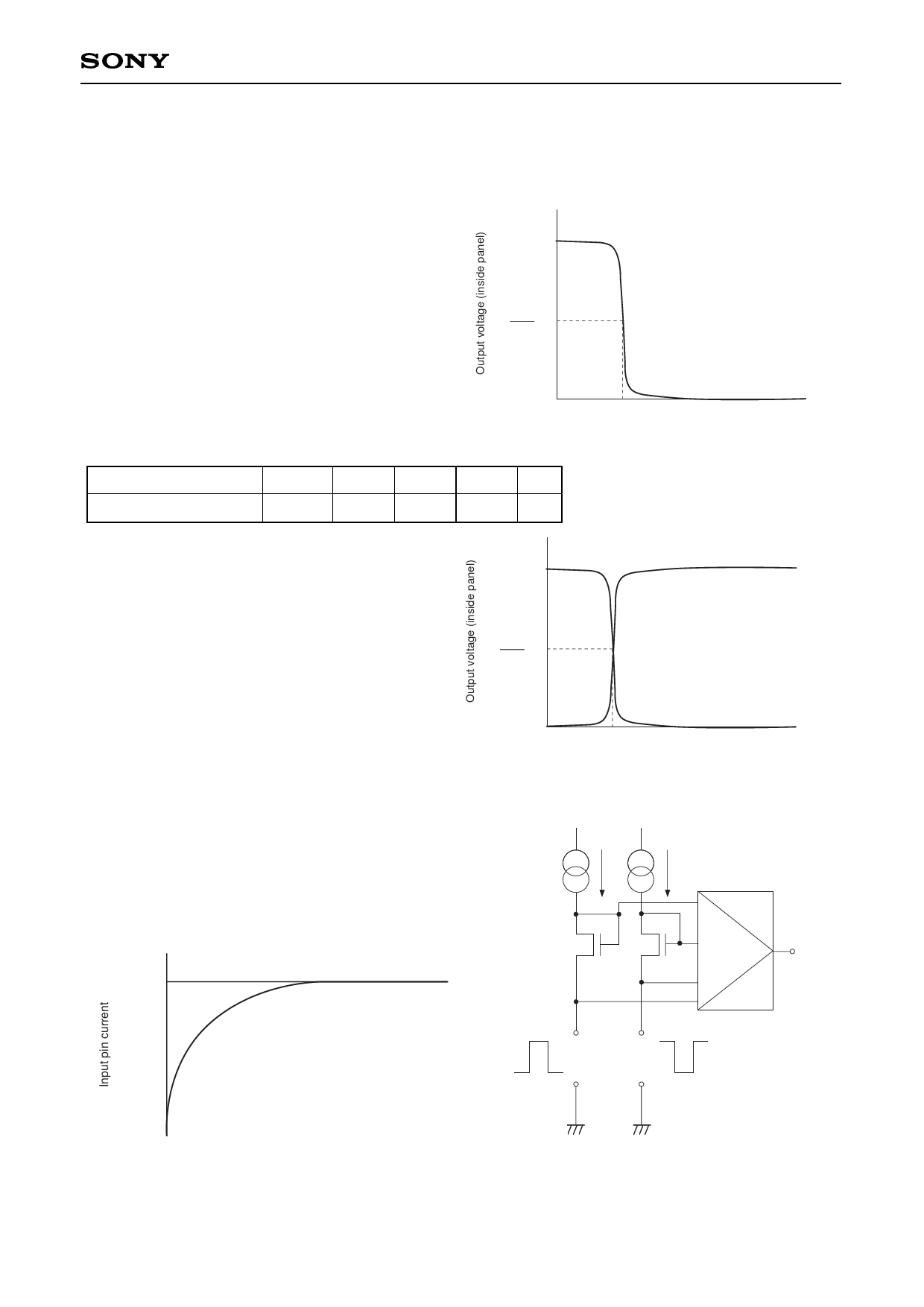
1. I/O characteristics of level conversion circuit
(For a single-phase input unit)
VDD
An example of the I/O voltage characteristics of a
level conversion circuit is shown in the figure to the
right. The input voltage value that becomes half the
output voltage (after voltage conversion) is defined
VDD
2
as Vth.
The Vth value varies depending on the VDD voltage.
The Vth values under standard conditions are
indicated in the table below. (HST, VST, EN, CLR,
RGT, VCK and BLK in the case of a single-phase input)
Item
Vth voltage of circuit
Symbol Min.
Vth
0.35
Typ.
1.50
VDD = 12.0V
Max. Unit
2.60 V
Example of single-phase
I/O characteristics
Vth
Input voltage [V]
VDD
(For a differential input unit)
An example of I/O voltage characteristics of a level
conversion circuit for a differential input is shown in
the figure to the right. Although the characteristics,
VDD
including those of the Vth voltage, are basically the
2
same as those for a single-phased input, the two-
phased input phase is defined. (Refer to clock
timing conditions.)
Vth
2. Current characteristics at the input pin of level conversion circuit
Example of differential I/O
characteristics
Input voltage [V]
A slight pull-in current is generated at the input pin
VDD
of the level conversion circuit. (The equivalent
circuit is shown to the right.) The current volume
increases as the voltage at the input pin decreases,
and is maximized when the pin is grounded. (Refer
to electrical characteristics.)
0
Input pin voltage [V]
10
0
output
Max. value
Pull-in current characteristics at the input pin
–5–
HCK1
input
HCK2
input
Level conversion equivalent circuit
Share Link: 