SL23EP08SC-3T 데이터 시트보기 (PDF) - Silicon Laboratories
부품명
상세내역
제조사
SL23EP08SC-3T Datasheet PDF : 15 Pages
| |||
SL23EP08
Low Jitter and Skew 10 to 220 MHz Zero Delay Buffer (ZDB)
Key Features
• 10 to 220 MHz operating frequency range
• Low output clock skew: 45ps-typ
• Low output clock jitter:
25 ps-typ cycle-to-cycle jitter
15 ps-typ period jitter
• Low part-to-part output skew: 90 ps-typ
• Wide 2.5 V to 3.3 V power supply range
• Low power dissipation:
20 mA-max at 66 MHz and VDD=3.3 V
18 mA-max at 66 MHz and VDD=2.5V
• One input drives 8 outputs
• Multiple configurations and drive options
• Select mode to bypass PLL or tri-state outputs
• SpreadThru™ PLL that allows use of SSCG
• Available in 16-pin SOIC and TSSOP packages
• Available in Commercial and Industrial grades
Applications
• Printers, MFPs and Digital Copiers
• PCs and Work Stations
• Routers, Switchers and Servers
• Datacom and Telecom
• High-SpeedDigital Embeded Systems
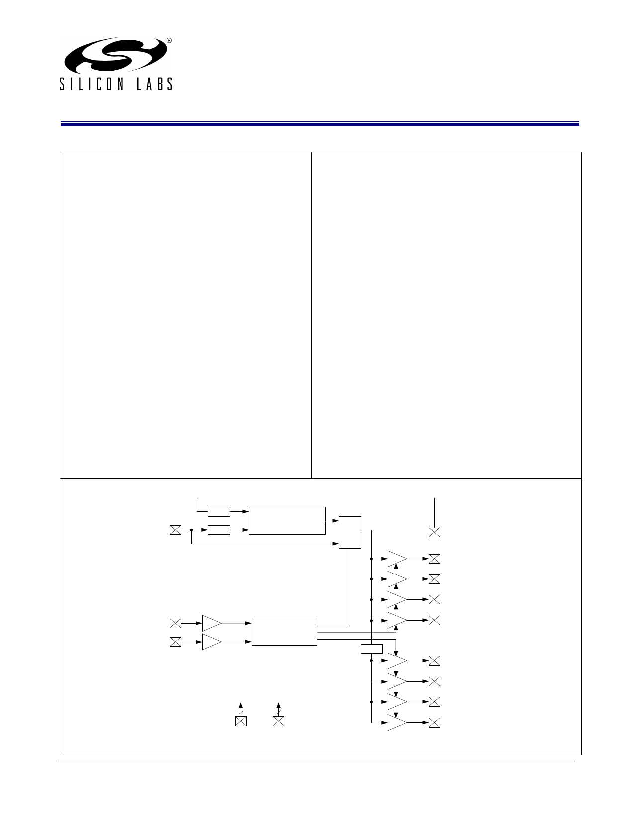
Block Diagram
Description
The SL23EP08 is a low skew, low jitter and low power Zero
Delay Buffer (ZDB) designed to produce up to nine (9) clock
outputs from one (1) reference input clock, for high speed
clock distribution applications.
The product has an on-chip PLL and a feedback pin (FBK)
which can be used to obtain feedback from any one of the
output clocks. The SL23EP08 has two (2) clock driver banks
each with four (4) clock outputs. These outputs are controlled
by two (2) select input pins S1 and S2. When only four (4)
outputs are needed, four (4) bank-B output clock buffers can
be tri-stated to reduce power dissipation and jitter. The select
inputs can also be used to tri-state both banks A and B or
drive them directly from the input bypassing the PLL and
making the product behave like a Non-Zero Delay Buffer
(NZDB). The product also offers various 1X, 2X and 4X
frequency options at the output clocks. Refer to the “Product
Configuration Table” for the details.
The high-drive version operates up to 220MHz and 200MHz at
3.3V and 2.5V power supplies respectively.
Benefits
• Up to eight (8) distribution of input clock
• Standard and High-Dirive levels to control impedance
level, frequency range and EMI
• Low power dissipation, jitter and skew
• Low cost
CLKIN
/2
(Divider for -3 and -4 only)
/2
(Divider for -5H only)
Low Power and
Low Jitter
PLL
MUX
FBK
CLKA1
CLKA2
CLKA3
S2
CLKA4
Input Selection
Decoding Logic
S1
/2
(Divider for -2 and -3 only)
CLKB1
2
VDD
2
GND
CLKB2
CLKB3
CLKB4
Rev 1.0, May 18, 2006
2400 West Cesar Chavez, Austin, TX 78701 1+(512) 416-8500
1+(512) 416-9669
Page 1 of 15
www.silabs.com
Share Link: 