NJM3774 데이터 시트보기 (PDF) - Japan Radio Corporation
부품명
상세내역
제조사
NJM3774 Datasheet PDF : 9 Pages
| |||
NJM3774
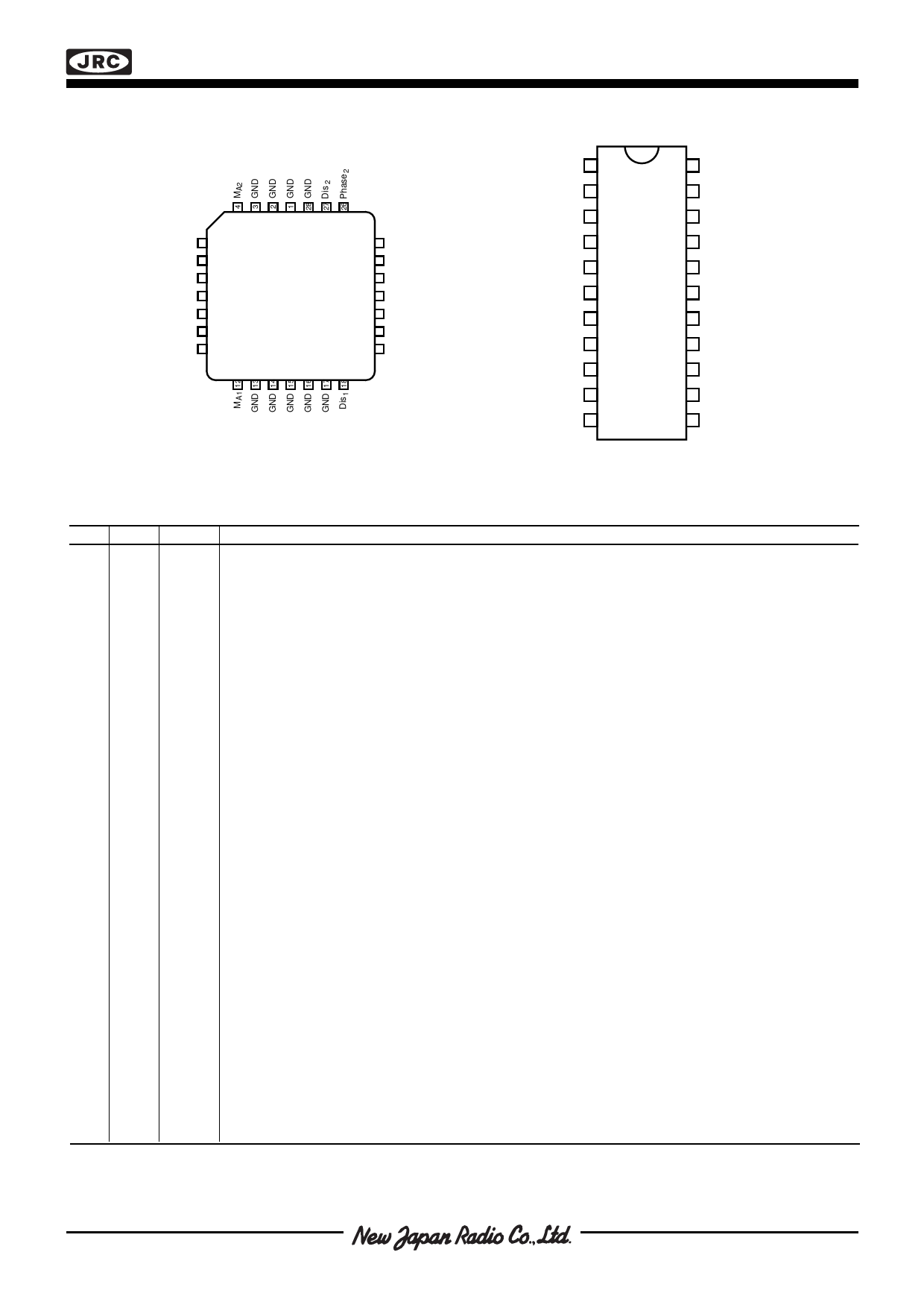
s PIN CONFIGURATIONS
VMM2 5
E2 6
M B2 7
M B1 8
GND 9
E1 10
VMM111
NJM3774FM2
25 VR2
24 C2
23 RC
22 VCC
21 C1
20 VR1
19 Phase1
RC 1
22 VCC
C2 2
21 C1
V R2 3
20 VR1
Phase 2 4
19 Phase1
GND 5
GND 6
Dis2 7
NJM
3774D2
18 GND
17 GND
16 Dis1
MA2 8
15 MA1
VMM2 9
14 VMM1
E2 10
MB2 11
13 E1
12 MB1
Figure 2. Pin configurations
s PIN DESCRIPTION
PLCC DIP
Symbol
1-3, 9, 5, 6 GND
13-17 17, 18
28
4
8
MA2
5
9
VMM2
6
10
E2
7
11
MB2
8
12 M
B1
10 13 E1
11
14
VMM1
12 15 M
A1
18 16 Dis1
19 19 Phase
1
20
20
VR1
21 21 C1
22
22
VCC
23 1
RC
24 2
C2
25 3
26 4
27 7
V
R2
Phase2
Dis2
Description
Ground and negative supply. Note: these pins are used thermally for heat-sinking. Make sure that all
ground pins are soldered onto a suitably large copper ground plane for efficient heat sinking.
Motor output A, channel 2. Motor current flows from MA2 to MB2 when Phase2 is HIGH.
Motor supply voltage, channel 2, +10 to +40 V.VMM1 and VMM2 should be connected together.
Common emitter, channel 2. This pin connects to a sensing resistor RS to ground.
Motor output B, channel 2. Motor current flows from MA2 to MB2 when Phase2 is HIGH.
Motor output B, channel 1. Motor current flows from M to M when Phase is HIGH.
A1
B1
1
Common emitter, channel 1. This pin connects to a sensing resistor RS to ground.
Motor supply voltage, channel 1, +10 to +40 V. VMM1 and VMM2 should be connected together.
Motor output A, channel 1. Motor current flows from M to M when Phase is HIGH.
A1
B1
1
Disable input (TTL level compatible) for channel 1. When HIGH, all four output transistors are turned
off, which results in a rapidly decreasing output current to zero.
Controls the direction of motor current at outputs M and M . Motor current flows from M to M
A1
B1
A1
B1
when Phase1 is HIGH.
Ref. voltage, channel 1. Controls the threshold voltage for the comparator and hence the output
current.
Comparator input channel 1. This input senses the instantaneous voltage across the sensing resistor,
filtered by an RC network. The threshold voltage for the comparator is V = 0.18 • V [V], i.e. 450
CH1
R1
mV at VR1 = 2.5 V.
Logic voltage supply, nominally +5 V.
Clock oscillator RC pin. Connect a 15 kohm resistor to V and a 3300 pF capacitor to ground to obtain
CC
the nominal switching frequency of 26.5 kHz.
Comparator input channel 2. This input senses the instantaneous voltage across the sensing resistor,
filtered by an RC network. The threshold voltage for the comparator is VCH2= 0.18 • VR2 [V], i.e. 450 mV
at VR2 = 2.5 V.
Ref. voltage, channel 2. Controls the threshold voltage for the comparator and hence the output
current.
Controls the direction of motor current at outputs MA2 and MB2. Motor current flows from MA2 to MB2
when Phase2 is HIGH.
Disable input (TTL level compatible) for channel 2. When HIGH, all four output transistors are turned
off, which results in a rapidly decreasing output current to zero.
Share Link: 