ZTX453 데이터 시트보기 (PDF) - Diodes Incorporated.
부품명
상세내역
제조사
ZTX453 Datasheet PDF : 5 Pages
| |||
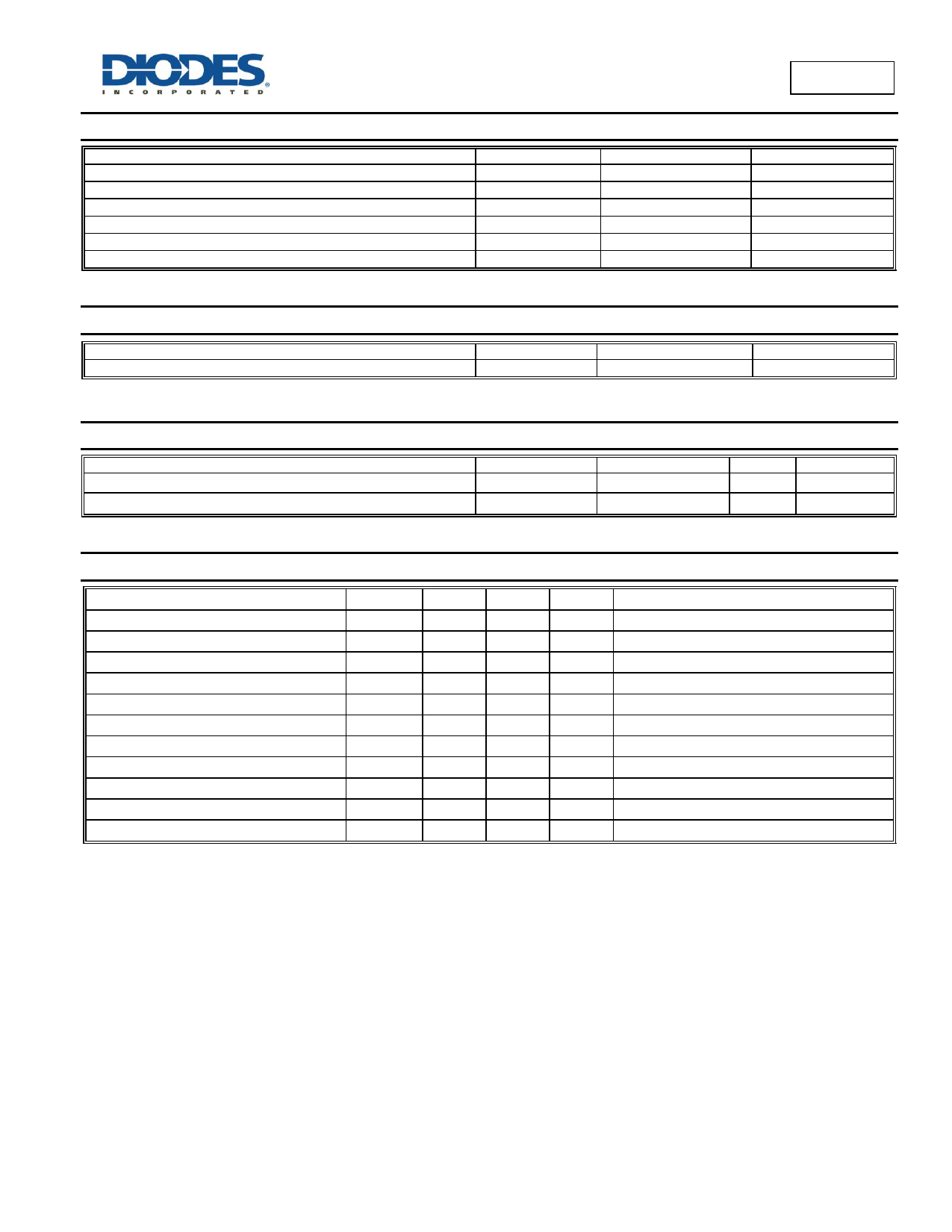
Maximum Ratings (@TA = +25°C, unless otherwise specified.)
Characteristic
Collector-Base Voltage
Collector-Emitter Voltage
Emitter-Base Voltage
Collector Current
Peak Collector Current
Peak Dissipation at TA = +25°C
Symbol
VCBO
VCEO
VEBO
IC
ICM
PD
Thermal Characteristics (@TA = +25°C, unless otherwise specified.)
Characteristic
Operating and Storage Temperature Range
Symbol
TJ, TSTG
Value
120
100
5
1
2
1
Value
-55 to +150
ZTX453
Unit
V
V
V
A
A
W
Unit
°C
ESD Ratings (Note 6)
Characteristic
Electrostatic Discharge - Human Body Model
Electrostatic Discharge - Machine Model
Symbol
ESD HBM
ESD MM
Value
8,000
400
Unit JEDEC Class
V
3B
V
C
Electrical Characteristics (@TA = +25°C, unless otherwise specified.)
Characteristic (Note 5)
Symbol
Min
Collector-Base Breakdown Voltage
BVCBO
120
Collector-Emitter Breakdown Voltage
BVCEO
100
Emitter-Base Breakdown Voltage
BVEBO
5
DC Current Gain
hFE
40
Collector-Emitter Saturation Voltage
VCE(SAT)
—
Base-Emitter Saturation Voltage
VBE(SAT)
—
Collector-Cutoff Current
ICBO
—
Emitter-Cutoff Current
IEBO
—
Gain Bandwidth Product
fT
150
Collector-Base Capacitance
CCBO
—
Output Capacitance
COBO
—
Notes:
5. Short duration pulse test used to minimize self-heating effect.
6. Refer to JEDEC specification JESD22-A114 and JESD22-A115.
Max
—
—
—
200
0.7
1.3
0.1
0.1
—
3.0
15
Unit
V
V
V
—
V
V
µA
µA
MHz
pF
pF
Test Condition
IC = 100µA, IB = 0
IC = 10mA, IB = 0
IE = 100µA, IC = 0
VCE = 10V, IC = 150mA, VCE = 10V, IC = 1A
IC = 150mA, IB = 15mA
IC = 150mA, IB = 15mA
VCB = 100V
VEB = 4V
VCE = 10V, IC = 50mA, f = 100MHz
VCB = 10V, f = 1MHz
VCB = 10V, f = 1MHz
ZTX453
Document number: DS33268 Rev. 3 - 2
2 of 5
www.diodes.com
November 2016
© Diodes Incorporated
Share Link: 