FSA1208 데이터 시트보기 (PDF) - ON Semiconductor
부품명
상세내역
제조사
FSA1208 Datasheet PDF : 9 Pages
| |||
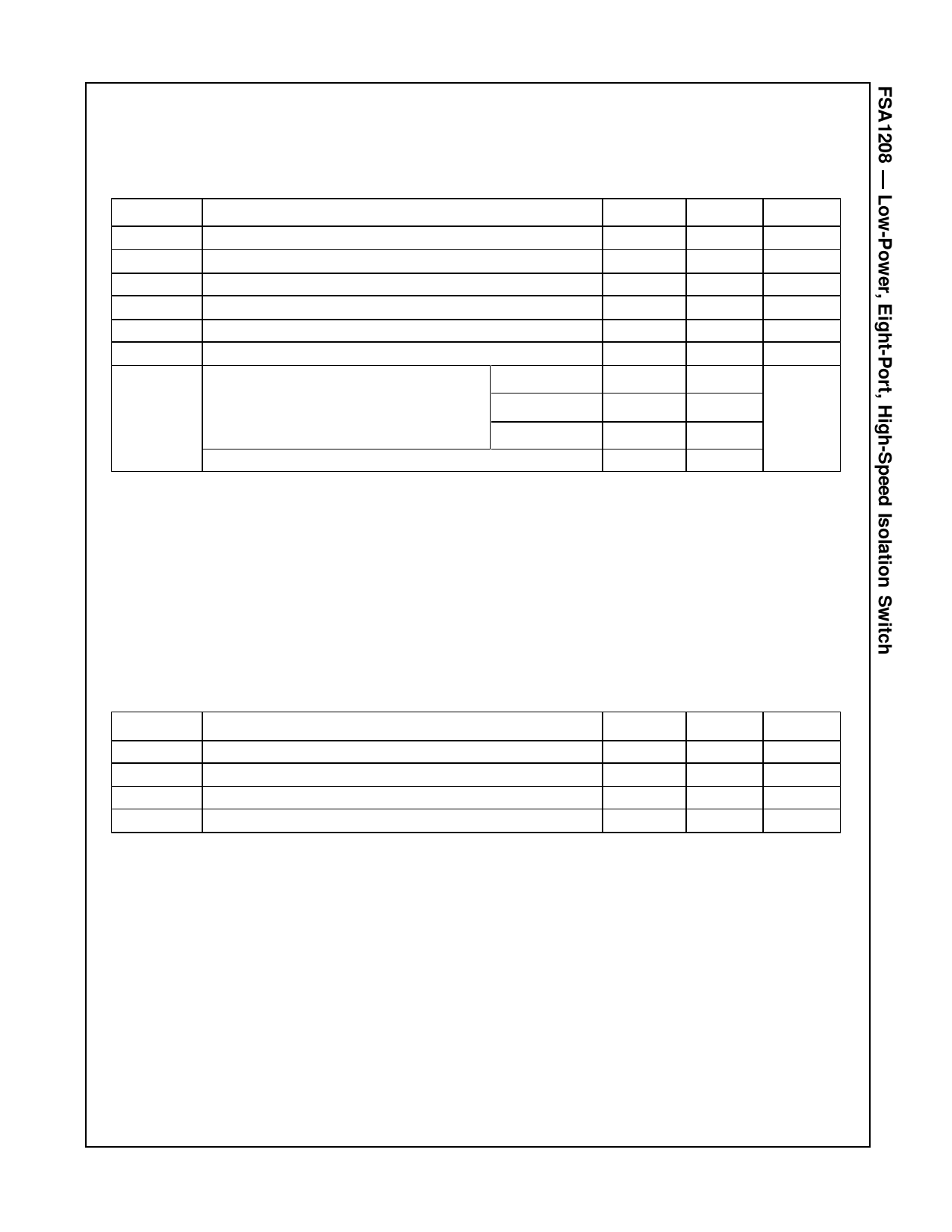
Absolute Maximum Ratings
Stresses exceeding the absolute maximum ratings may damage the device. The device may not function or be
operable above the recommended operating conditions and stressing the parts to these levels is not recommended.
In addition, extended exposure to stresses above the recommended operating conditions may affect device reliability.
The absolute maximum ratings are stress ratings only.
Symbol
VCC
VCNTRL
V SW
IIK
IOUT
TSTG
Parameter
Supply Voltage
DC Input Voltage (/OE)(1)
DC Sw itch I/O Voltage(1)
DC Input Diode Current
DC Output Current
Storage Temperature
All Pins
Min.
-0.50
-0.50
-0.50
-50
-65
Max.
+5.25
VCC
5.25
50
+150
7.5
Unit
V
V
V
mA
mA
°C
Human Body Model, JEDEC: JESD22-A114 I/O to GND
ESD
Pow er to GND
8
kV
16
Charged Device Model, JEDEC: JESD22-C101
2
Note :
1. The input and output negative ratings may be exceeded if the input and output diode current ratings are
observed.
Recommended Operating Conditions
The Recommended Operating Conditions table defines the conditions for actual device operation. Recommended
operating conditions are specified to ensure optimal performance to the datasheet specifications. ON Semiconductor
does not recommend exceeding them or designing to Absolute Maximum Ratings.
Symbol
Parameter
VCC
V
(2)
CNTRL
Supply Voltage
Control Input Voltage (S, /OE)
V SW
Sw itch I/O Voltage
TA
Operating Temperature
Note :
2. The control input must be held HIGH or LOW; it must not float.
Min.
2.3
0
-0.5
-40
Max.
4.3
VCC
VCC
+85
Unit
V
V
V
°C
www.onsemi.com
3
Share Link: 