MAX3679A 데이터 시트보기 (PDF) - Microsemi Corporation
부품명
상세내역
제조사
MAX3679A Datasheet PDF : 12 Pages
| |||
+3.3V, Low-Jitter Crystal to LVPECL
Clock Generator
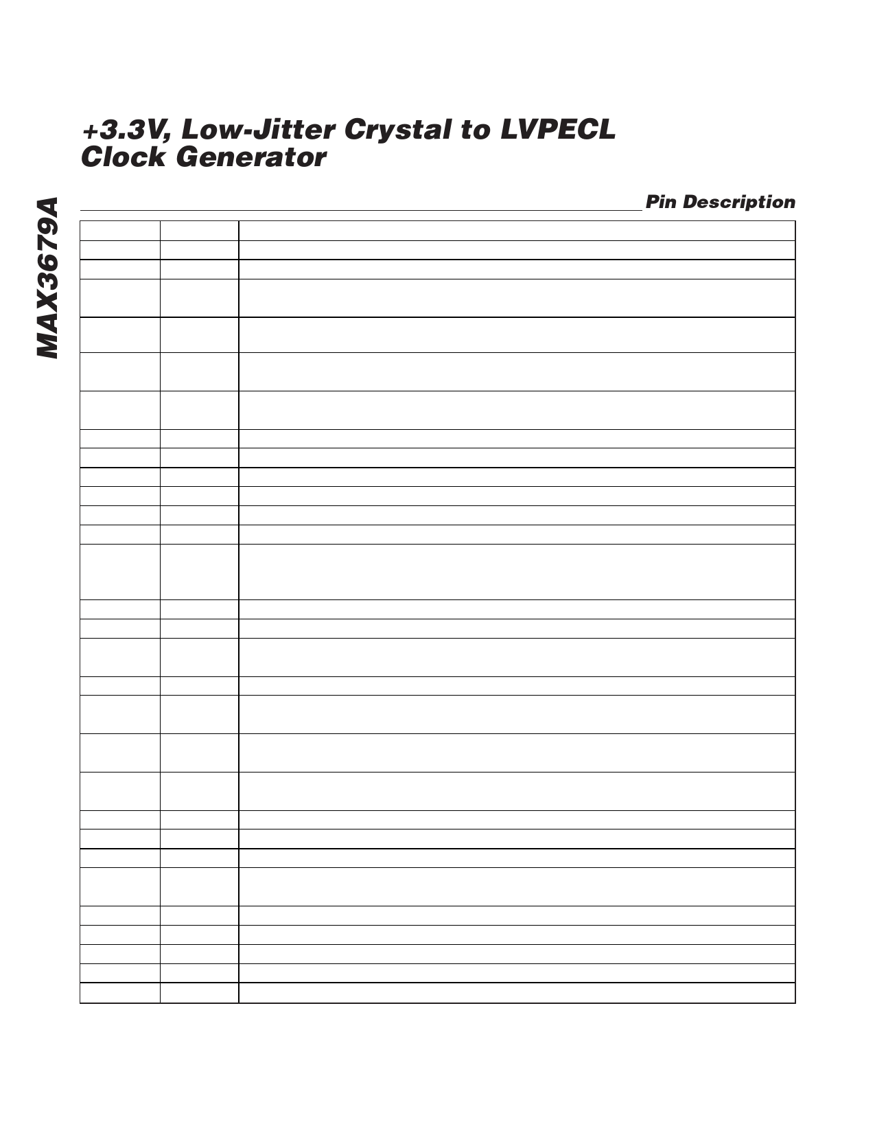
PIN
1
2, 19, 24
3
4, 5
6
7
8
9
10
11
12
13
14
15
16
17
18
20
21, 22
23
25
26
27
28
29
30
31
32
—
Pin Description
NAME
VCCO_B
GND
QB0_OE
SELB1,
SELB0
QAC_OE
MR
GNDO_A
QA_C
VDDO_A
VCCO_A
QA
QA
BYPASS
RES1
RES0
VCCA
VCC
QA_OE
SELA0,
SELA1
QB1_OE
X_OUT
X_IN
REF_IN
IN_SEL
QB1
QB1
QB0
QB0
EP
FUNCTION
Power Supply for QB0 and QB1 Clock Outputs. Connect to +3.3V.
Supply Ground
LVCMOS/LVTTL Input. Enables/disables QB0 clock output. Connect pin high to enable LVPECL
clock output QB0. Connect low to set QB0 to a logic 0. Has internal 50k input impedance.
LVCMOS/LVTTL Input. Controls NB divider setting. Has 50k input impedance. See Table 2 for
more information.
LVCMOS/LVTTL Input. Enables/disables QA_C clock output. Connect pin high to enable QA_C.
Connect low to set QA_C to a high-impedance state. Has internal 75k pullup to VCC.
LVCMOS/LVTTL Input. Master reset input. Pulse high for > 1μs to reset all dividers. Has internal
75k pulldown to GND. Not required for normal operation.
Ground for QA_C Output. Connect to supply ground.
LVCMOS Clock Output
Power Supply for QA_C Clock Output. Connect to +3.3V.
Power Supply for QA Clock Output. Connect to +3.3V.
Noninverting Clock Output, LVPECL
Inverting Clock Output, LVPECL
LVCMOS/LVTTL Input (Active Low). Connect low to bypass the internal PLL. Connect high for
normal operation. When in bypass mode the output dividers are set to divide by 1. Has internal
75k pullup to VCC.
Not Internally Connected. Connect to GND, VCC, or leave open for normal operation.
Reserved for Test. Connect to GND for normal operation.
Analog Power Supply for the VCO. Connect to +3.3V. For additional power-supply noise filtering,
this pin can connect to VCC through 10.5 as shown in Figure 2 (requires VCC = +3.3V ±5%).
Core Power Supply. Connect to +3.3V.
LVCMOS/LVTTL Input. Enables/disables the QA clock output. Connect this pin high to enable the
LVPECL clock output QA. Connect low to set QA to a logic 0. Has internal 75k pullup to VCC.
LVCMOS/LVTTL Input. Controls NA divider setting. See Table 2 for more information. Has 50k
input impedance.
LVCMOS/LVTTL Input. Enables/disables QB1 clock output. Connect pin high to enable LVPECL
clock output QB1. Connect low to set QB1 to a logic 0. Has internal 50k input impedance.
Crystal Oscillator Output
Crystal Oscillator Input
LVCMOS Reference Clock Input. Self-biased to allow AC- or DC-coupling.
LVCMOS/LVTTL Input. Connect high or leave open to use a crystal. Connect low to use REF_IN.
Has internal 75k pullup to VCC.
LVPECL, Inverting Clock Output
LVPECL, Noninverting Clock Output
LVPECL, Inverting Clock Output
LVPECL, Noninverting Clock Output
Exposed Pad. Connect to supply ground for proper electrical and thermal performance.
6 _______________________________________________________________________________________
Share Link: 