ARA05050 데이터 시트보기 (PDF) - Skyworks Solutions
부품명
상세내역
제조사
ARA05050 Datasheet PDF : 16 Pages
| |||
ARA05050
APPLICATION INFORMATION
Printed Circuit Board Layout Considerations
The ARA05050 is a high-performance RF device.
Special consideration must be given to certain features
of the the printed circuit board layout, as they can affect
the RF performance of the IC. Refer to the application
note “CATV Reverse Amp w/ Step Attenuator” for
more details.
Thermal Layout Considerations
The device package for the ARA05050 features a
heat slug on the bottom of the package body. Use of
the heat slug is an integral part of the device design.
Soldering it to the ground plane of the PC board will
ensure the lowest possible thermal resistance for the
device, and will result in the longest MTF (mean time
to failure.)
Amplifier Enable / Disable
The ARA05050 includes two amplification stages
that each can be shut down through external control
pins Vref1 and Vref2 (pins 5 and 19, respectively.)
By applying a typical bias of 1.75 Volts to these pins,
the amplifiers are enabled. In order to fully disable
an amplifier, its control pin requires a negative bias
of -1.5 to -2.0 Volts.
Amplifier Bias Current
The Iset pins (11 and 25) set the bias current for the
amplification stages. Grounding these pins results
in the maximum possible current. By placing a
resistor from the pin to ground, the current can be
reduced. The recommended bias conditions use the
configuration shown in the test circuit schematic in
Figure 4.
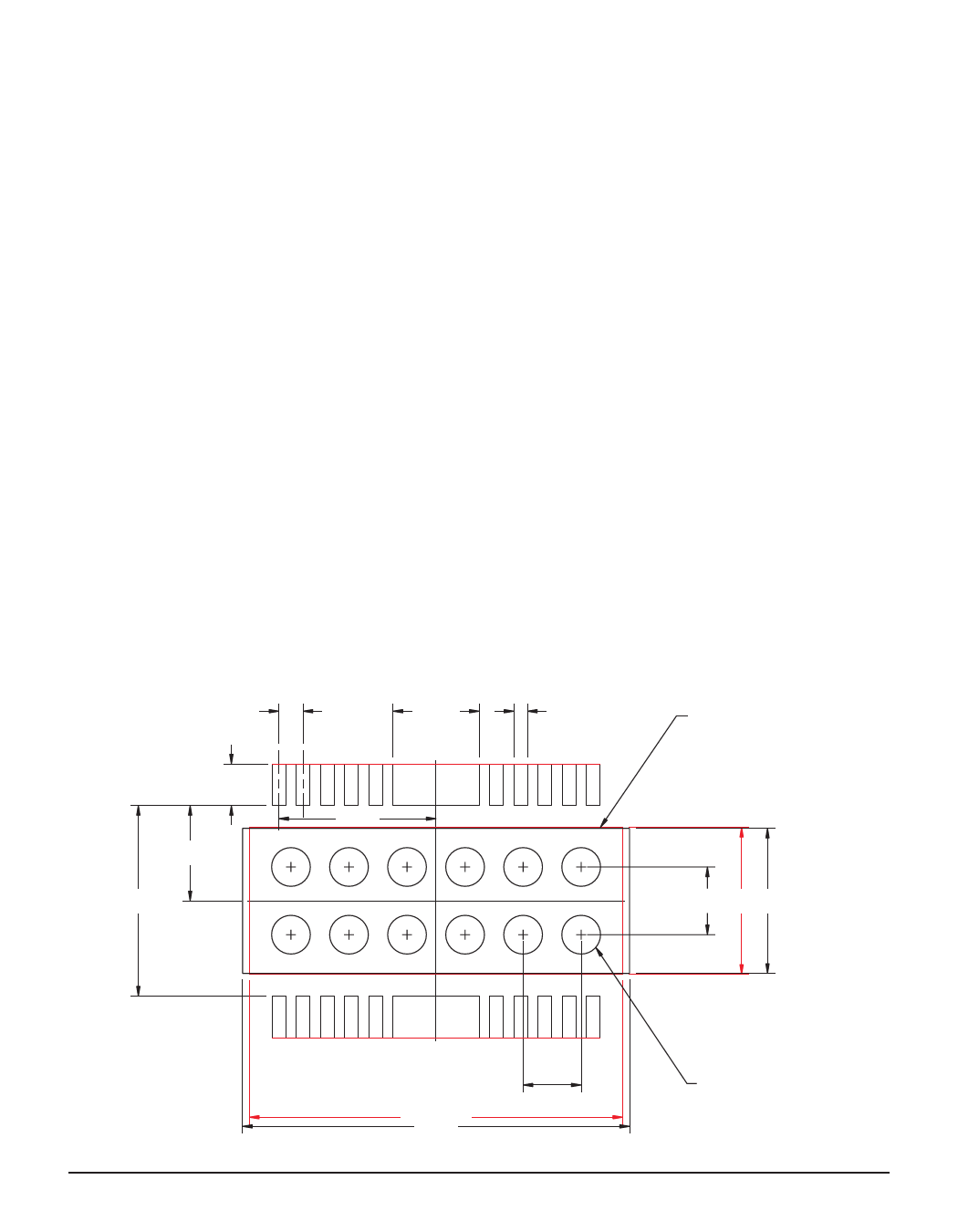
A PC board layout that optimizes the benefits of the
heat slug is shown in Figure 13. The via holes located
under the body of the device must be plated through
to a ground plane layer of metal, in order to provide
sufficient thermal conductivity. The recommended
solder mask outline is shown in Figure 14.
ESD Sensitivity
Electrostatic discharges can cause permanent damage
to this device. Electrostatic charges accumulate
on test equipment and the human body, and can
discharge without detection. Proper precautions and
handling are strongly recommended. Refer to the
application note on ESD precautions.
0.025 BSC
0.089
0.014 TY P
BODY OUTLIN E
(NOMINAL )
0.025 MIN.
0.099
0.197
0.163
0.070
0.152
REF .
0.150
0.060 TY P.
0.386 REF .
0.400
Figure 13: PC Board Layout
(12X)0.020 TO 0.060 DIA. P
PLA TED THRU HOLES.
10
Data Sheet
September 19, 2016 • Skyworks Proprietary and Confidential Information • Products and Product Information are Subject to Change Without Notice • 204227B
Share Link: 