SMJ27C010A-20JM 데이터 시트보기 (PDF) - Micross Components
부품명
상세내역
제조사
SMJ27C010A-20JM Datasheet PDF : 13 Pages
| |||
UVEPROM
SMJ27C010A
AS27C010A
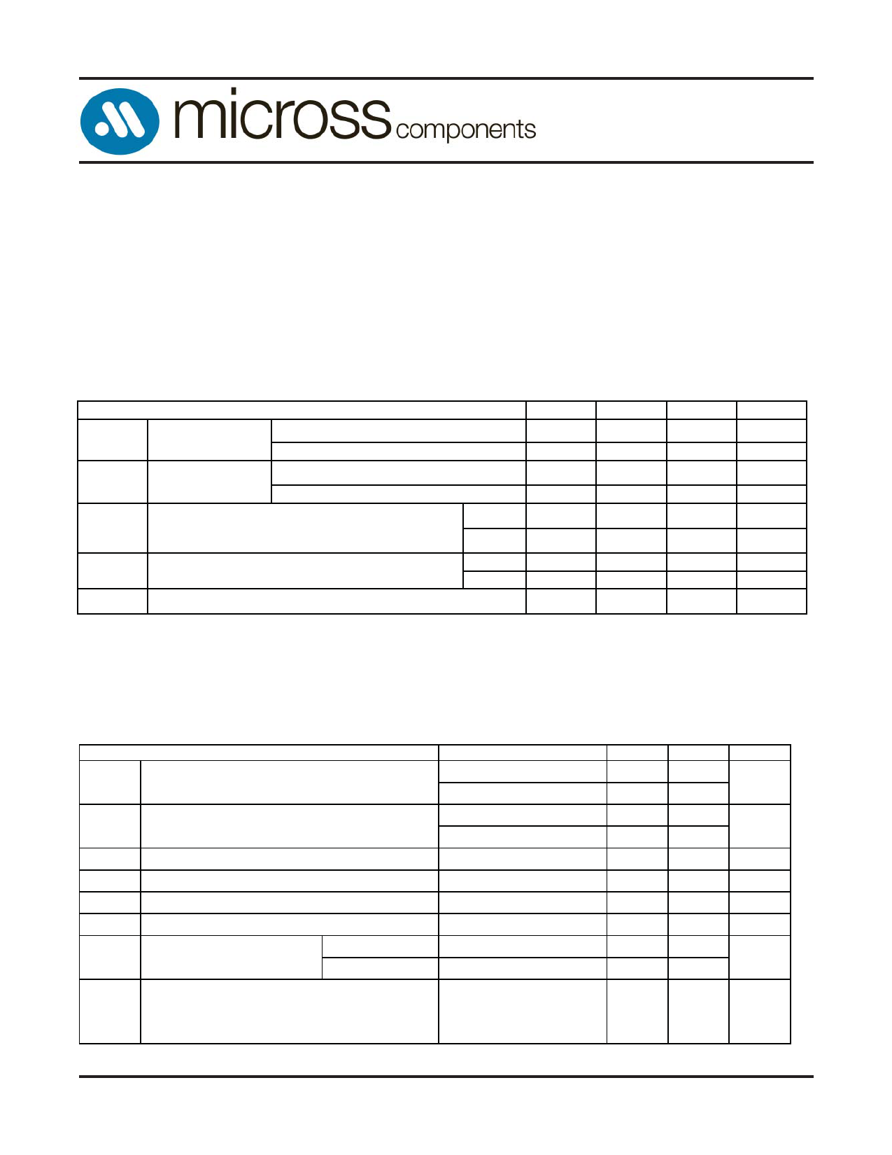
ABSOLUTE MAXIMUM RATINGS*
*Stresses greater than those listed under “Absolute Maximum
Supply Voltage Range, VCC**...........................-0.6V to +7.0V
Supply Voltage Range, Vpp**.........................-0.6V to +14.0V
Ratings” may cause permanent damage to the device. This is a
stress rating only and functional operation of the device at these
or any other conditions above those indicated in the operation
Input Voltage Range, All inputs except A9**..-0.6V to VCC+1 section of this specification is not implied.
Exposure to
A9.....-0.6V to +13.5V absolute maximum rating conditions for extended periods may
Output Voltage Range,
affect reliability.
with respect to VSS**..................................-0.6V to VCC +1 ** All voltage values are with respect to GND.
Operating Free-air Temperature Range, TA....-55°C to 125°C
Storage Temperature Range, Tstg.....................-65°C to 150°C
RECOMMENDED OPERATING CONDITIONS
VCC Supply Voltage
VPP Supply Voltage
Read Mode1
SNAP! Pulse programming algorithm
Read Mode2
SNAP! Pulse programming algorithm
MIN
4.5
6.25
VCC-0.6
12.75
NOM
5
6.5
VCC
13
MAX
5.5
6.75
VCC+0.6
13.25
UNIT
V
V
V
V
VIH High-level DC input voltage
VIL Low-level DC input voltage
TTL
CMOS
TTL
CMOS
2
VCC-0.2
-0.5
-0.5
VCC+0.5
V
VCC+0.5
V
0.8
V
GND+0.2 V
TA
NOTES:
Operating free-air temperature
-55
125
°C
1. VCC must be applied before or at the same time as VPP and removed after or at the same time as VPP. The deivce must not be inserted into or removed from
the board when VPP or VCC is applied.
2. During programming, VPP must be maintained at 13V ± 0.25V.
ELECTRICAL CHARACTERISTICS OVER RECOMMENDED RANGES OF SUPPLY VOLTAGE AND
OPERATING FREE-AIR TEMPERATURE
PARAMETER
TEST CONDITIONS
MIN
MAX UNIT
VOH High-level DC output voltage
IOH = -20μA
IOH = -2.5mA
VCC-0.2
V
3.5
VOL Low-level DC output voltage
II Input current (leakage)
IO Output current (leakage)
IOL = 2.1mA
IOL = 20μA
VI = 0V to 5.5V
VO = 0V to VCC
0.4
V
0.1
±1
μA
±1
μA
IPP1 VPP supply current
VPP = VCC = 5.5V
10
μA
IPP2 VPP supply current (during program pulse)
VPP = 13V
50
mA
TTL-Input Level
ICC1 VCC supply current (standby)
VCC = 5.5V, E\=VIH
CMOS-Input Level VCC = 5.5V, E\=VCC±0.2V
500
μA
100
ICC2 VCC supply current (active) (output open)
E\=VIL, VCC=5.5V
tcycle = minimum cycle time,
outputs open1
30
mA
NOTES:
1. Minimum cycle time = maximum access time.
SMJ27C010A
AS27C010A
Rev. 2.6 01/10
Micross Components reserves the right to change products or specifications without notice.
5
Share Link: 