NT7181F 데이터 시트보기 (PDF) - Novatek Microelectronics
부품명
상세내역
제조사
NT7181F Datasheet PDF : 15 Pages
| |||
4 Absolute Maximum Ratings
Supply voltage range, VCC (see Note1)……………………………………………………..-0.3V to 4V
Output voltage range, VO…..……………….…………………………………………………-0.3V to VCC +0.3V
Input voltage range, VI……………………………….……………………….…………………………-0.3V to Vcc +0.3V
Storage temperature range, Tstg……………………………………………………………-65°C to 150°C
Lead temperature 1, 6 mm (1/16 inch) from case for 10 seconds………………………260°C
Junction Temperature…………………………………………………………………………150°C
# Stresses above those listed under "Absolute Maximum Ratings" may cause permanent damage to this device. These are stress
ratings only. Functional operation of this device at these or any other conditions above those indicated in the operational sections of
this specification is not implied or intended. Exposure to the absolute maximum rating conditions for extended periods may affect
device reliability.
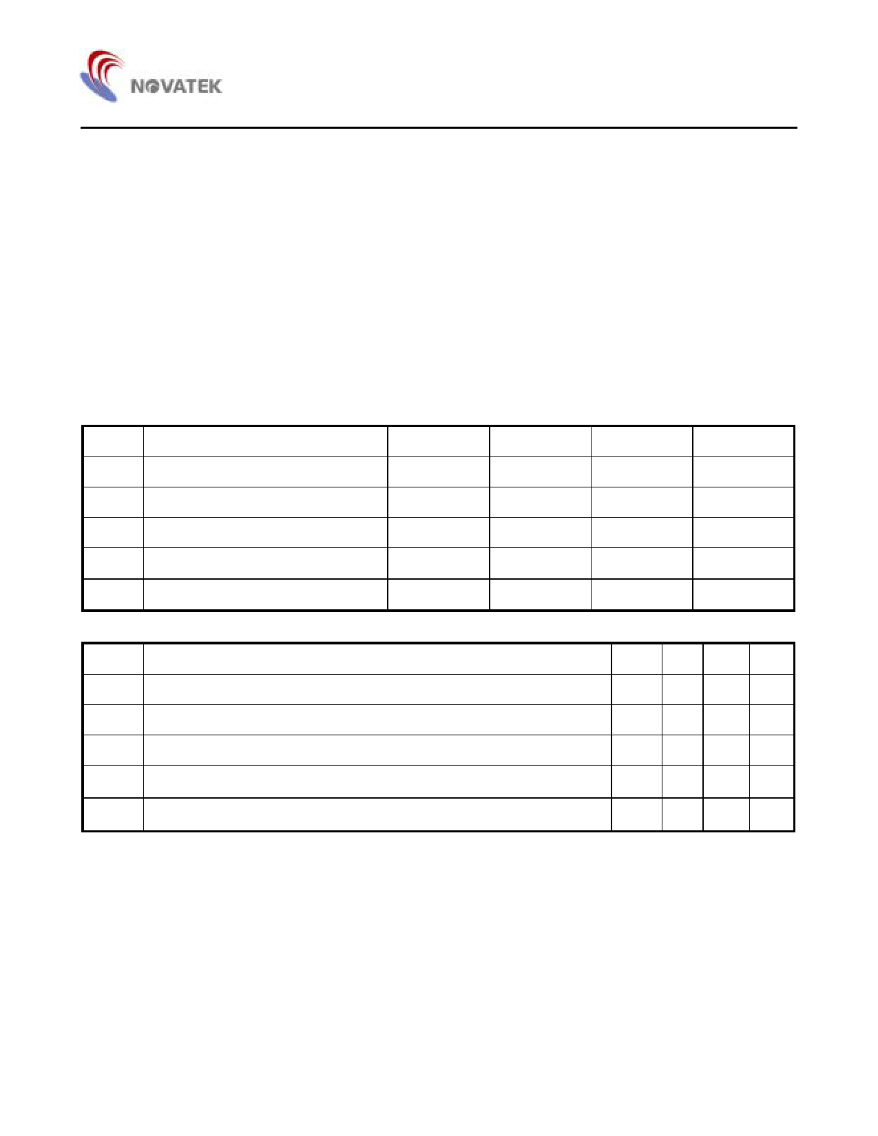
4.1 Recommended Operating Conditions
Symbol
Parameter
VCC Supply voltage
VIH
High-level input voltage
VIL
Low-level input voltage
ZL
Differential load impedance
TA
Operating free-air temperature
Min.
Nom.
Max.
Unit
3.0
3.3
3.6
V
2
V
0.8
V
90
100
110
Ω
0
70
°C
4.2 Timing requirements
Symbol
Parameter
Min. Nom. Max. Unit
TC
Cycle time, input clock
11.8
40 ns
tW
Pulse duration, high-level input clock
0.4tc
0.6tc ns
tT
Transition,
5
ns
tsu
Setup time, data, TD0 - TD27 valid before CLKIN↑or CLKIN ↓ (See Figure 1)
5
ns
th
Hold time, data, , TD0 - TD27 valid after CLKIN↑or CLKIN ↓ (See Figure 1)
2.5
ns
Note: th is measured under the conditions of input clock jitter of 1.9ns at 65MHz.
5
Share Link: 