BTB08 데이터 시트보기 (PDF) - Foshan Blue Rocket Electronics Co.,Ltd.
부품명
상세내역
제조사
BTB08 Datasheet PDF : 8 Pages
| |||
BTB08
Rev.D Nov.-2015
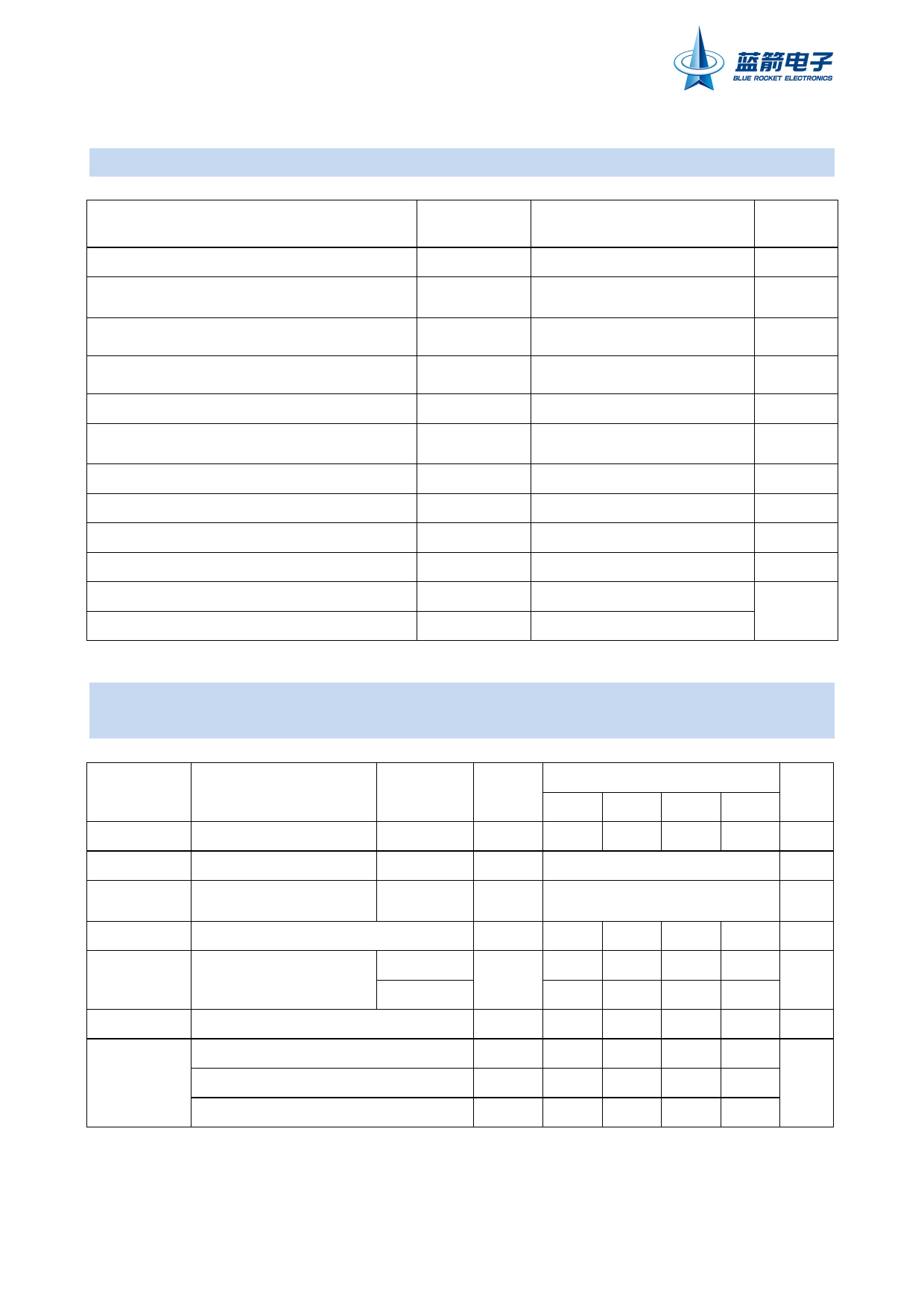
极限参数 / Absolute Maximum Ratings(Ta=25℃)
参数
Parameter
Repetitive peak off-state voltages
On-state rms current(full sine wave
TC=105℃)
Non repetitive surge peak on-state
current(full cycle, Tj initial=25°C)
Non repetitive surge peak on-state
current(full cycle, Tj initial=25°C)
I2t value for fusing
Critical rate of rise of on-state current
IG =2xIGT, tr≤100 ns(F=120Hz Tj=125℃)
Peak gate current(tp =20μs Tj=125℃)
Average gate power dissipation(Tj=125℃)
Operating junction temperature range
Storage junction temperature range
Junction to ambient
Junction to case for AC
符号
Symbol
VDRM/VRRM
IT(RMS)
ITSM(F=50Hz
t=20ms)
ITSM(F=60Hz
t=16.7ms)
I2t(tp=10ms)
dI/dt
IGM
PG(AV)
Tj
Tstg
Rth(j-a)
Rth(j-c)
DATA SHEET
数值
Rating
600/700
8
80
84
36
50
4.0
1.0
-40~125
-40~150
60
1.6
单位
Unit
V
A
A
A
A2s
A/μs
A
W
℃
℃
℃ /W
电性能参数 / Electrical Characteristics(Ta=25℃)
免缓冲器和逻辑电平(3象限) / Snubberless and logic level(3 quadrants)
符号
Symbol
IGT(1)
VGT
VGD
IH(2)
IL
(dV/dt)(2)
(dI/dt)c(2)
测试条件
Test Conditions
信号区
Quadrant
VD=12V RL=30Ω
I-II-III
VD=12V RL=30Ω
VD=VDRM RL=3.3KΩ
Tj=125℃
IT=100mA
I-II-III
I-II-III
I-III
IG=1.2IGT
II
VD=67% VDRM gate open Tj=125℃
(dV/dt)c=0.1V/μs Tj=125℃
(dV/dt)c=10V/μs Tj=125℃
Without snubber Tj=125℃
Max.
Max.
Min.
Max.
Max.
Min.
Min.
Min.
Min.
Note 1:minimum IGT is guaranted at 5% of IGT max.
Note 2:for both polarities of A2 referenced to A1.
BTB08
单位
TW SW CW BW Unit
5
10 35 50 mA
1.3
V
0.2
V
10 15 35 50 mA
10 25 50 70
mA
15 30 60 80
20 40 400 1000 V/μs
3.5 5.4
-
-
1.5 2.98 -
- A/ms
-
-
4.5
7
http://www.fsbrec.com
2/8
Share Link: 