LV8014T 데이터 시트보기 (PDF) - ON Semiconductor
부품명
상세내역
제조사
LV8014T Datasheet PDF : 6 Pages
| |||
LV8014T
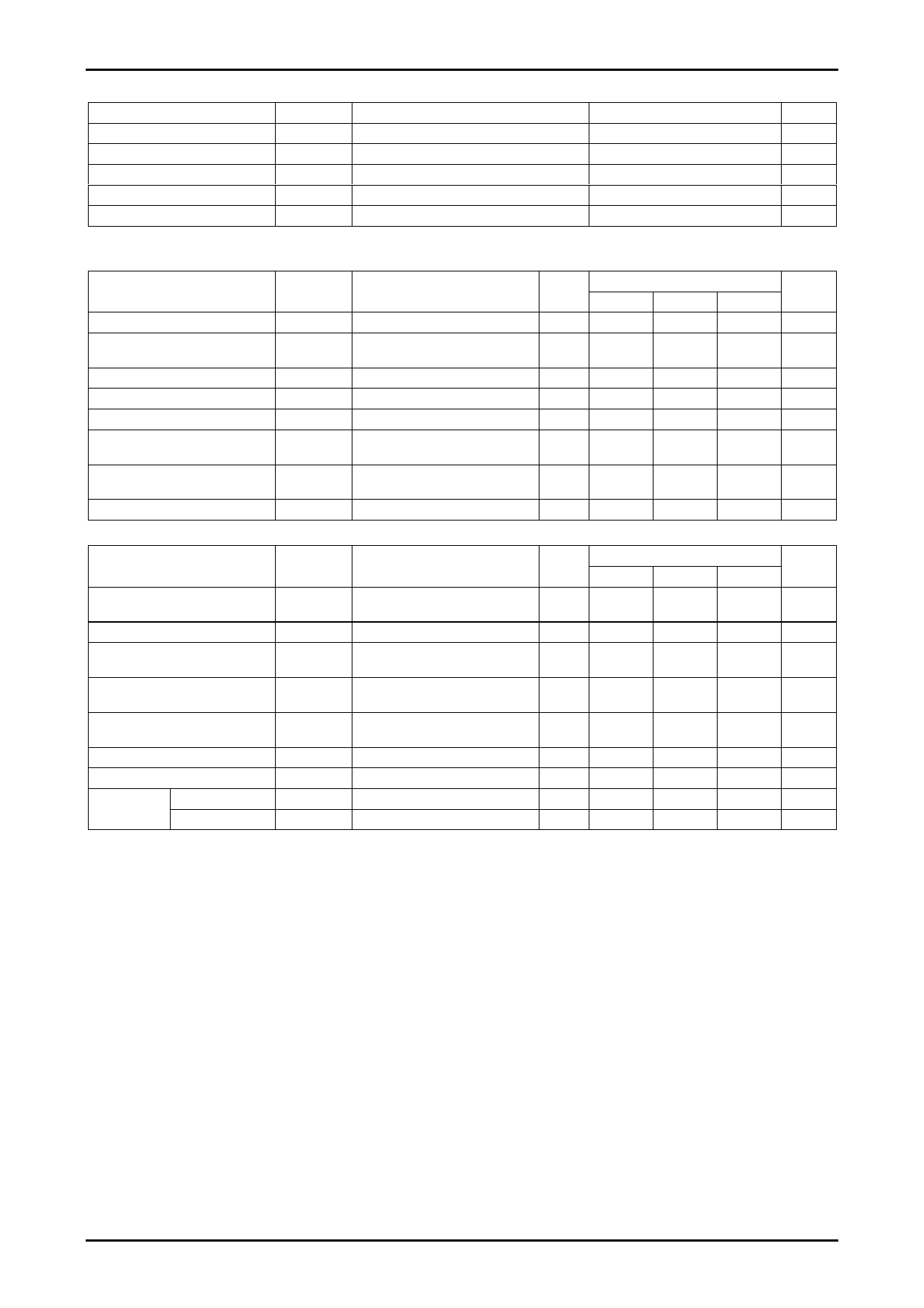
Allowable Operating Ratings at Ta = 25°C, SGND = PGND = 0V
Parameter
Supply voltage (VM Pin)
Supply voltage (VCC Pin)
Input signal voltage
Input signal frequenc
Capacitor for charge pump
Symbol
VM
VCC
VIN
f max
C1, C2, C3
Conditions
Ratings
Unit
2.0 to 7.0
V
2.7 to 5.5
V
0 to VCC
V
100 kHz
0.001 to 0.1
μF
Electrical Characteristics at Ta = 25°C, VCC = VM1 = VM2 = 5.0V, SGND = PGND = 0V, unless especially specified.
Parameter
Supply current for load at standby
Symbol
IMO
Conditions
EN = 0V
Remarks
min
1
Ratings
typ
Unit
max
1.0
μA
Supply current for control at
ICO
EN = 0V,
2
standby
IN1 = IN2 = IN3 = IN4 = 0V
Current drain during operation
IC1
EN = 5V, VG at no load
3
1.0
μA
0.7
1.2
mA
H-level input voltage
L-level input voltage
H-level input current
(IN1, IN2, IN3, IN4)
L-level input current
(IN1, IN2, IN3, IN4)
Pull-down resistance (EN1, 2)
VIH
VIL
IIH
IIL
RUP
2.7V ≤ VCC ≤ 5.5V
2.7V ≤ VCC ≤ 5.5V
0.6×VCC
0
4
4
-1.0
100
VCC
V
0.2×VCC
V
1.0
μA
μA
200
400
kΩ
Ta = 25°C, VCC = VM = 5.0V, SGND = PGND = 0V
Parameter
Symbol
Conditions
Ratings
Remarks
Unit
min
typ
max
Output ON resistance
Charge pump voltage
RON
Sum of ON resistances at top and
5
bottom
VG
6
0.75
1.2
Ω
8.5
10.5
V
Low-voltage detection operation
voltage
Thermal shutdown operation
temperature
Charge pump capacity
(IG = 500μA)
IG current dissipation (Fin = 20kHz)
VCS
Tth
VGLOAD
IG
7
2.15
2.30
2.45
V
8
180
°C
9
8
9
V
10
350
μA
Charge pump start time
TVG
CVG = 0.1μF
11
1.0
ms
Output block Turn on time
TPLH
12
0.2
0.4
μs
Turn off time
TPHL
12
0.2
0.4
μs
Remarks
1. It shows current dissipation of VM1, VM2 pin in output OFF state.
2. It shows current dissipation of VCC pin in stand-by state.
(The standard current depends on EN pin pull-down resistance.)
3. It shows current dissipation of VCC pin in state of EN = 5V (stand-by), including current dissipation of VG pin.
4. For IN1, IN2, IN3 and IN4 pins, no pull-down and pull-up resistance is needed. (High impedance pin)
5. It shows sum of upper and lower saturation voltages of OUT pin.
6. It controls charge-pump oscillation and makes specified voltage.
7. When low voltage is detected, the lower output is turned OFF.
8. When thermal protection circuit is activated, the lower output is turned OFF.
When the heat temperature is fallen, it is turned ON again.
9. IG (VG pin load current) = 500μA
10. It shows VG pin current dissipation in state of PWM input for IN pin.
11. It specifies start-up time from 10% to 90% when VG is in non-load state
(when setting the capacitor between VG and GND to 0.1μF and VCC is 5V).
12. It specifies 10% to 90% for start-up and 90% to 10% for shut-down.
No. A1134-2/6
Share Link: 