LB1860 데이터 시트보기 (PDF) - ON Semiconductor
부품명
상세내역
제조사
LB1860 Datasheet PDF : 8 Pages
| |||
LB1860,1860M,1861,1861M
. From this relation, it can be observed that the ‘to’ and ‘ton’ are in proportional relation with each other, and that the ‘ton/to’
equals the ‘on’ time duty. As a result, a certain rotation speed can be fixed despite the fact that rotation speed exclusively
. depends on each motor.
At the start, the ‘ton’ value becomes longer while the ‘toff’ value remains unchanged. This means that the ‘toff/to’ duty becomes
small enough compared to normal rotation mode. Therefore, the same start torque as that of the full speed rotation can be
obtained because the ‘on’ operation time duty increases. This enables the motor to start at a very low speed.
.(2) Supply voltage (VIN pin)
The LB1860 has the internal parallel regulator which supplies power to the Hall amplifier circuit and the control block.
Therefore, the driver ICs are not affected by power source fluctuations and kickbacks from the motor. They maintain the stable
. operations even if noise signals such as surge are generated.
Set the resistance R1 between VCC and VIN so that the ICC current of 6 mA to 50 mA can flow onto the VIN pin within the
supply voltage range of a fan motor.
. VIN is 6.7 V typ at ICC = 7 mA.
. The current flowing into VIN is calculated using the equation shown below.
ICC =
VCC – VIN
............................ 2
R1
. Consideration given to surge voltage
. The maximum allowable current at VIN pin is 200 mA. Therefore, the pin is designed to withstand abnormal positive voltage of:
Vsurge = VIN + R1 × 200 mA ............................................ 3
.(3) Hall input pin voltage (Pins IN–, IN+)
Set the voltage levels of the input pin for the Hall element output and the Hall element output voltage to within the range of
. 0 V to VIN – 1.5 V.
The gain between the hall input pin and the output pin is 100 dB or greater. The offset voltage of the hall input amp is ±7 mV,
therefore, the hall element output must be set with the offset voltage (±7 mV) considered.
(4) Output transistor (Pins OUT1, OUT2)
. Output current
. Output saturation voltage
. Output limiting voltage
IO = 1.5 A max
VO sat = 1.15 V/1.0 A typ
VOLM = 57 V typ (LB1860, 1860M)
. VOLM = 32 V typ (LB1861,1861M)
Since the LB1860 series have a protect zener diode between collector and base, the kickback voltage induced by the coil is cut
at VOLM = 57 V (32 V). When external capacitors are connected between OUT and GND, the capacitance should not exceed
10 µF.
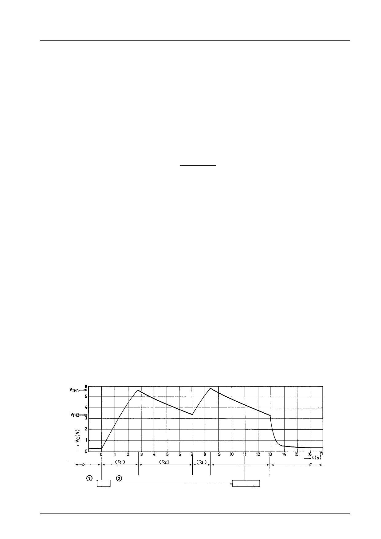
(5) Output protection function (C pin)
. Capacitor pin used in forming an automatic return circuit.
. If rotation is stopped due to overload, the pin voltage level increases and then forces the output to become inactive. In this case,
after proper load adjustment, the output returns to the ‘drive’ mode from the ‘stop’ mode automatically. By changing the
capacitor value, the lock detect time period can be set.
For C marked with 1 µF
Lock detect time
Approximately 2 sec.
Lock protect time (output ON) Approximately 1 sec.
(output OFF) Approximately 6 sec.
Rotation Output ON
Lock
Output OFF
Output
ON
Output OFF
Lock release
Automatic Return Circuit C Pin Voltage
Rotation
No.4
Share Link: 