HV219FG-GM931 데이터 시트보기 (PDF) - Supertex Inc
부품명
상세내역
제조사
HV219FG-GM931 Datasheet PDF : 9 Pages
| |||
Ordering Information
Part Number
Package Option
HV219FG-G
HV219FG-G M931
48-Lead LQFP
HV219PJ-G
HV219PJ-G M904
28-Lead PLCC
-G denotes a lead (Pb)-free / RoHS compliant package
Packing
250/Tray
1000/Reel
38/Tube
500/Reel
Absolute Maximum Ratings
Parameter
Value
VDD logic power supply voltage
VPP - VNN supply voltage
VPP positive high voltage supply
VNN negative high voltage supply
Logic input voltages
Analog signal range
Peak analog signal current/channel
-0.5V to +15V
220V
-0.5V to VNN +200V
+0.5V to -200V
-0.5V to VDD +0.3V
VNN to VPP
3.0A
Storage temperature
-65OC to +150OC
Power dissipation:
28-Lead PLCC
48-Lead LQFP
1.2W
1.0W
Absolute Maximum Ratings are those values beyond which damage to the device may occur.
Functional operation under these conditions is not implied. Continuous operation of the device
at the absolute rating level may affect device reliability. All voltages are referenced to device
ground.
Operating Conditions
Sym Parameter
VDD Logic power supply voltage
VPP Positive high voltage supply
VNN Negative high voltage supply
VIH High level input logic voltage
VIL Low-level input logic voltage
VSIG
Analog signal voltage
peak-to-peak
TA Operating free air temperature
Value
4.5V to 13.2V
40V to VNN +200V
-40V to -160V
VDD -1.5V to VDD
0V to 1.5V
VNN +10V to VPP -10V
0OC to 70OC
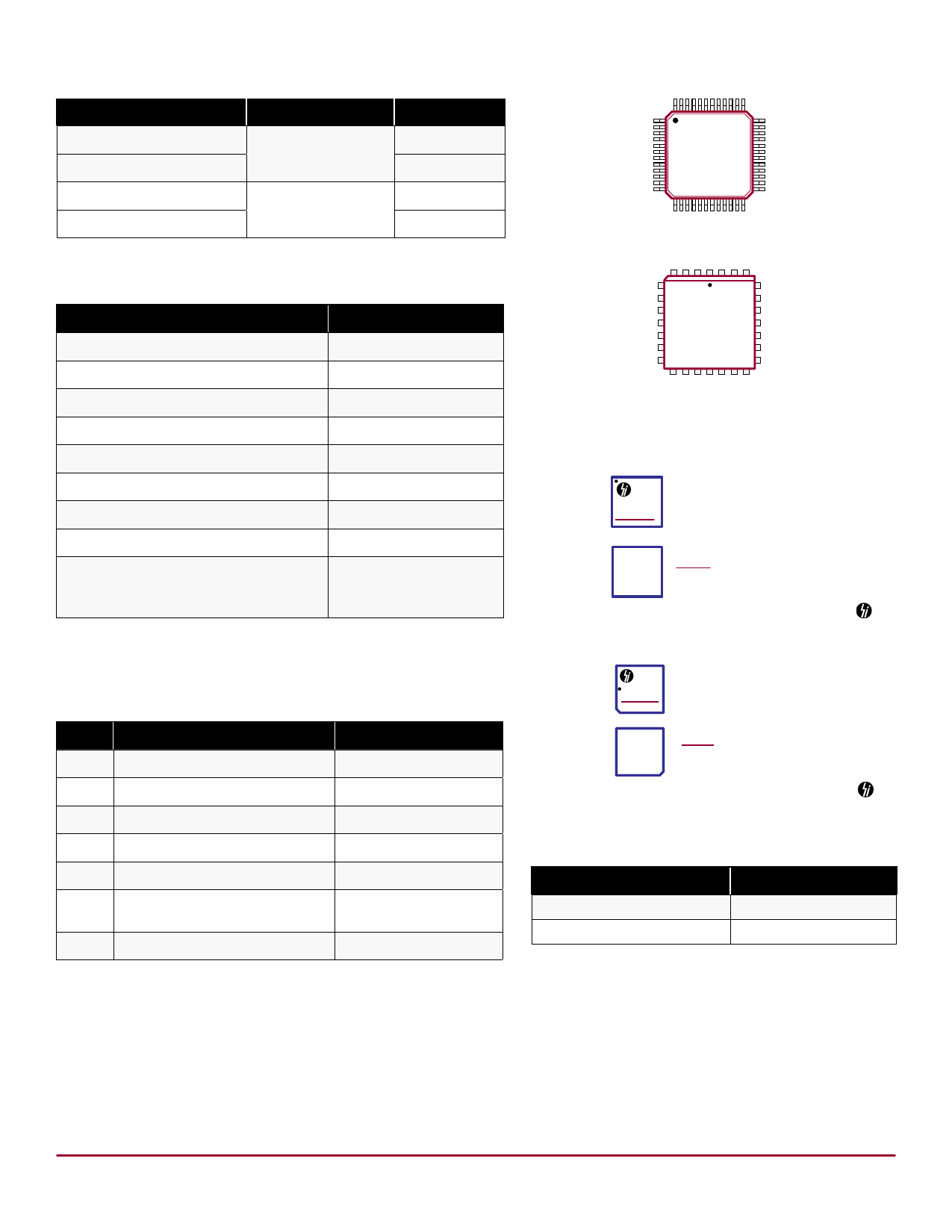
Pin Configuration
48
1
HV219
48-Lead LQFP
(top view)
4
1 28 26
28-Lead PLCC
(top view)
Product Marking
Top Marking
YYWW
HV219FG
LLLLLLLLL
YY = Year Sealed
WW = Week Sealed
L = Lot Number
Bottom Marking C = Country of Origin*
A = Assembler ID*
CCCCCCCC
AAA
= “Green” Packaging
*May be part of top marking
Package may or may not include the following marks: Si or
48-Lead LQFP
Top Marking
YYWW
HV219PJ
LLLLLLLLLL
YY = Year Sealed
WW = Week Sealed
L = Lot Number
Bottom Marking
C = Country of Origin*
A = Assembler ID*
CCCCCCCCCCC
AAA
= “Green” Packaging
*May be part of top marking
Package may or may not include the following marks: Si or
28-Lead PLCC
Typical Thermal Resistance
Package
48-Lead LQFP
θja
52OC/W
28-Lead PLCC
48OC/W
Power Up/Down Sequence
1. Power up/down sequence is arbitrary except GND must be powered up first and powered down last. This applies for
applications powering GND of the IC with different voltages.
2. VSIG must always be at or in between VPP and VNN or floating during power up/down transition.
3. Rise and fall times of the power supplies VDD, VPP, and VNN should not be less than 1.0ms.
Doc.# DSFP-HV219
C070713
Supertex inc.
2
www.supertex.com
Share Link: 