AP1120(2009) 데이터 시트보기 (PDF) - Diodes Incorporated.
부품명
상세내역
제조사
AP1120 Datasheet PDF : 7 Pages
| |||
AP1120
DUAL 1A LOW DROPOUT POSITIVE REGULATOR
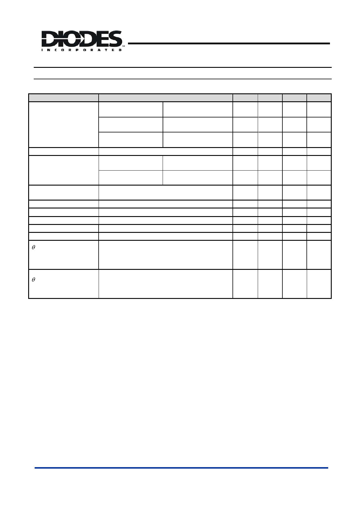
Absolute Maximum Ratings
Symbol
VIN
PD
TST
TOP
Parameter
DC Supply Voltage
Power Dissipation
Storage Temperature
Operating Junction Temperature Range
Rating
-0.3 to 18 V
Internally Limited
-65 to +150
0 to +150
Unit
V
oC
oC
Electrical Characteristics (Under Operating Conditions)
Parameter
Conditions
Output Voltage
AP1120(B) - VOUT1
AP1120 - VOUT2
AP1120B - VOUT2
IOUT = 10mA, TA = 25oC,
4.8V≦VIN≦12V
IOUT = 10mA, TA = 25oC,
4V≦VIN≦12V
IOUT = 10mA, TA = 25oC,
4V≦VIN≦12V
Line Regulation
IO=10mA,VOUT+1.5V<VIN<12V, TA =25oC
Load Regulation
AP1120 series
VOUT1
AP1120 series
VOUT2
VIN = 5V, 0≦IOUT≦1A,
TA =25oC (Note 3, 4)
VIN=4V, 0mA<Io<1A,
TA =25oC (Note 3, 4)
Dropout Voltage
(VIN-VOUT)
IOUT = 1A,ΔVOUT=0.1%VOUT
Current Limit
(VIN-VOUT) = 5V
Minimum Load Current 0oC≦Tj≦125oC (Note 5)
Thermal Regulation
TA=25 oC, 30ms pulse
Ripple Rejection
F=120Hz,COUT=25uF Tantalum, IOUT=1A
Temperature Stability IO=10mA
θ JA Thermal Resistance
SOP-8L: Control Circuitry/Power Transistor
(Note 6)
Junction-to-Ambient (No CH1 or CH2 only
heat sink; No air flow) CH1 & CH2 and PD1=PD2
Min
3.235
2.450
1.764
1. 1
Typ.
3.300
2.500
1.800
26
20
1.3
5
0.008
60
0.5
50
45
Max
3.365
2.550
1.836
0.2
33
25
1.4
10
0.04
70
SOP-8L: Control Circuitry/Power Transistor
θ JC Thermal Resistance (Note 6)
Junction-to-Case
CH1 or CH2 only
CH1 & CH2 and PD1=PD2
20
12
Notes:
3. See thermal regulation specifications for changes in output voltage due to heating effects. Line and load regulation are
measured at a constant junction temperature by low duty cycle pulse testing. Load regulation is measured at the output
lead = 1/18” from the package.
4. Line and load regulation are guaranteed up to the maximum power dissipation of 15W. Power dissipation is determined by
the input/output differentially and the output current. Guaranteed maximum power dissipation will not be available over the
full input/output range.
5. Quiescent current is defined as the minimum output current that requires maintaining regulation. At 12V input/output
differential the device is guaranteed to regulate if the output current is greater than 10mA.
6. Vout1 and Vout2 are connected to the PCB copper area 5.5mm*5.5mm separately. If you need large PD or lower Tc & Tj,
please connect to the large copper area >> 5.5mm*5.5mm (like 10mm*10mm).
Unit
V
V
V
%
mV
mV
V
A
mA
%/W
dB
%
OC/W
OC/W
AP1120 Rev. 2
4 of 7
www.diodes.com
FEBRUARY 2009
© Diodes Incorporated
Share Link: 