EL8108 데이터 시트보기 (PDF) - Renesas Electronics
부품명
상세내역
제조사
EL8108 Datasheet PDF : 14 Pages
| |||
EL8108
Absolute Maximum Ratings (TA = +25°C)
VS+ Voltage to Ground . . . . . . . . . . . . . . . . . . . . . . -0.3V to +13.2V
VIN+ Voltage . . . . . . . . . . . . . . . . . . . . . . . . . . . . . . . . . GND to VS+
Current into any Input . . . . . . . . . . . . . . . . . . . . . . . . . . . . . . . . 8mA
Continuous Output Current . . . . . . . . . . . . . . . . . . . . . . . . . . . 75mA
Thermal Information
Ambient Operating Temperature Range . . . . . . . . . .-40°C to +85°C
Storage Temperature Range . . . . . . . . . . . . . . . . . .-60°C to +150°C
Operating Junction Temperature . . . . . . . . . . . . . . . . . . . . . . +150°C
Power Dissipation . . . . . . . . . . . . . . . . . . . . . . . . . . . . . See Curves
Pb-free Reflow Profile . . . . . . . . . . . . . . . . . . . . . . . . .see link below
http://www.intersil.com/pbfree/Pb-FreeReflow.asp
CAUTION: Do not operate at or near the maximum ratings listed for extended periods of time. Exposure to such conditions may adversely impact product reliability and
result in failures not covered by warranty.
IMPORTANT NOTE: All parameters having Min/Max specifications are guaranteed. Typical values are for information purposes only. Unless otherwise noted, all tests
are at the specified temperature and are pulsed tests, therefore: TJ = TC = TA
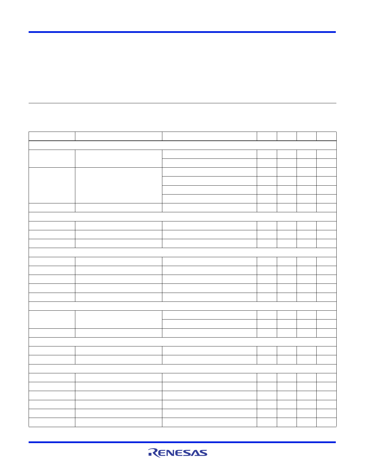
Electrical Specifications VS = 12V, RF = 750, RL = 100 connected to mid supply, TA = +25°C, unless otherwise specified.
PARAMETER
DESCRIPTION
CONDITIONS
MIN TYP MAX UNIT
AC PERFORMANCE
BW
-3dB Bandwidth
HD
Total Harmonic Distortion, Differential
SR
Slew Rate, Single-ended
DC PERFORMANCE
RF = 500, AV = +2
RF = 500, AV = +4
f = 200kHz, VO = 16VP-P, RL = 50
f = 4MHz, VO = 2VP-P, RL = 100
f = 8MHz, VO = 2VP-P, RL = 100
f = 16MHz, VO = 2VP-P, RL = 100
VOUT from -3V to +3V
200
MHz
150
MHz
-72
-83
dBc
-70
dBc
-60
dBc
-50
dBc
600
800 1100 V/µs
VOS
Offset Voltage
VOS
VOS Mismatch
ROL
Transimpedance
INPUT CHARACTERISTICS
VOUT from -4.5V to +4.5V
-25
+25
mV
-3
+3
mV
0.7
1.4
2.5
M
IB+
Non-inverting Input Bias Current
IB-
Inverting Input Bias Current
IB-
IB- Mismatch
eN
Input Noise Voltage
iN
-Input Noise Current
OUTPUT CHARACTERISTICS
-5
5
µA
-20
5
+20
µA
-18
0
+18
µA
6
nV Hz
13
pA/ Hz
VOUT
IOUT
SUPPLY
Loaded Output Swing (Single-ended)
Output Current
VS = ±6V, RL = 100 to GND
VS = ±6V, RL = 25to GND
RL = 0
±4.8
±5
V
±4.7
V
450
mA
VS
Supply Voltage
IS (EL8108IS only) Supply Current, Maximum Setting
SUPPLY (EL8108IL ONLY)
Single supply
All outputs at mid supply
4.5
13
V
11
14.3
18
mA
IS+ (Full Power)
Positive Supply Current per Amplifier
IS+ (Medium Power) Positive Supply Current per Amplifier
IS+ (Low Power)
Positive Supply Current per Amplifier
IS+ (Power Down) Positive Supply Current per Amplifier
IINH, C0 or C1
C0, C1 Input Current, High
IINL, C0 or C1
C0, C1 Input Current, Low
All outputs at 0V, C0 = C1 = 0V
All outputs at 0V, C0 = 5V, C1 = 0V
All outputs at 0V, C0 = 0V, C1 = 5V
All outputs at 0V, C0 = C1 = 5V
C0, C1 = 5V
C0, C1 = 0V
11
14.3
18
mA
7
8.9
11
mA
3.7
4.5
5.5
mA
0.1
0.5
mA
90
125
160
µA
-5
+5
µA
FN7417 Rev 2.00
January 29, 2008
Page 3 of 14
Share Link: 