ISL12023 데이터 시트보기 (PDF) - Renesas Electronics
부품명
상세내역
제조사
ISL12023
Renesas Electronics

ISL12023 Datasheet PDF : 29 Pages
| |||
ISL12023
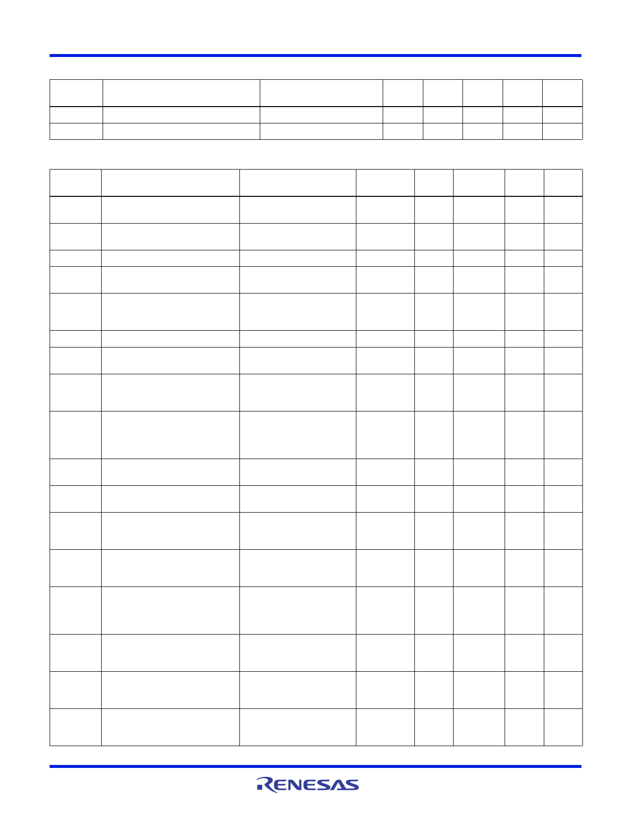
Power-Down Timing Test Conditions: VDD = +2.7 to +5.5V, TA = -40°C to +85°C, unless otherwise stated.
SYMBOL
PARAMETER
CONDITIONS
MIN
TYP
MAX
(Note 11) (Note 7) (Note 11) UNITS
VDD SR-
VDDSR+
VDD Negative Slew Rate
VDD Positive Slew Rate, Minimum
10
V/ms
0.05
V/ms
I2C Interface Specifications Test Conditions: VDD = +2.7 to +5.5V, TA = -40°C to +85°C, unless otherwise specified.
SYMBOL
PARAMETER
TEST CONDITIONS
MIN
(Note 11)
TYP
MAX
(Note 7) (Note 11)
UNITS
VIL
SDA and SCL Input Buffer LOW
Voltage
-0.3
0.3 x VDD
V
VIH
SDA and SCL Input Buffer HIGH
Voltage
0.7 x VDD
VDD + 0.3
V
Hysteresis SDA and SCL Input Buffer Hysteresis
VOL
SDA Output Buffer LOW Voltage,
Sinking 3mA
VDD = 5V, IOL = 3mA
0.05 x VDD
V
0
0.02
0.4
V
CPIN
SDA and SCL Pin Capacitance
TA = +25°C, f = 1MHz,
VDD = 5V, VIN = 0V,
VOUT = 0V
fSCL
SCL Frequency
tIN
Pulse Width Suppression Time at SDA Any pulse narrower than the
and SCL Inputs
max spec is suppressed.
10
pF
400
kHz
50
ns
tAA
SCL Falling Edge To SDA Output Data SCL falling edge crossing 30%
Valid
of VDD, until SDA exits the 30%
to 70% of VDD window.
tBUF
Time the Bus must be Free Before the SDA crossing 70% of VDD
Start of a New Transmission
during a STOP condition, to SDA
crossing 70% of VDD during the
following START condition.
1300
900
ns
ns
tLOW
Clock LOW Time
Measured at the 30% of VDD
1300
ns
crossing.
tHIGH Clock HIGH Time
Measured at the 70% of VDD
600
ns
crossing.
tSU:STA START Condition Setup Time
tHD:STA START Condition Hold Time
tSU:DAT Input Data Setup Time
tHD:DAT Input Data Hold Time
tSU:STO STOP Condition Setup Time
tHD:STO STOP Condition Hold Time
SCL rising edge to SDA falling
600
edge. Both crossing 70% of
VDD.
From SDA falling edge crossing
600
30% of VDD to SCL falling edge
crossing 70% of VDD.
From SDA exiting the 30% to
100
70% of VDD window, to SCL
rising edge crossing 30% of
VDD.
From SCL falling edge crossing
0
30% of VDD to SDA entering the
30% to 70% of VDD window.
From SCL rising edge crossing
600
70% of VDD, to SDA rising edge
crossing 30% of VDD.
From SDA rising edge to SCL
600
falling edge. Both crossing 70%
of VDD.
ns
ns
ns
900
ns
ns
ns
NOTES
8
14
NOTES
9, 10
9, 10
FN6682 Rev 3.00
December 6, 2011
Page 4 of 29
Share Link: