ISL12023 데이터 시트보기 (PDF) - Renesas Electronics
부품명
상세내역
제조사
ISL12023
Renesas Electronics

ISL12023 Datasheet PDF : 29 Pages
| |||
ISL12023
I2C Interface Specifications Test Conditions: VDD = +2.7 to +5.5V, TA = -40°C to +85°C, unless otherwise specified. (Continued)
SYMBOL
PARAMETER
TEST CONDITIONS
MIN
(Note 11)
TYP
MAX
(Note 7) (Note 11)
UNITS NOTES
tDH
Output Data Hold Time
From SCL falling edge crossing
0
30% of VDD, until SDA enters
the 30% to 70% of VDD window.
tR
SDA and SCL Rise Time
From 30% to 70% of VDD.
20 + 0.1 x Cb
tF
SDA and SCL Fall Time
From 70% to 30% of VDD.
20 + 0.1 x Cb
Cb
Capacitive Loading of SDA or SCL Total on-chip and off-chip
10
300
300
400
ns
ns
10
ns
10
pF
10
RPU
SDA and SCL Bus Pull-up Resistor Off- Maximum is determined by tR
1
chip
and tF.
For Cb = 400pF, max is about
2k~2.5k.
For Cb = 40pF, max is about
15k~20k
k
10
NOTES:
4. Temperature Conversion is inactive below VBAT = 2.7V. Device operation is not guaranteed at VBAT<1.8V.
5. IRQ/FOUT Inactive.
6. VDD > VBAT +VBATHYS
7. Specified at +25°C.
8. In order to ensure proper timekeeping, the VDD SR- specification must be followed.
9. Limits should be considered typical and are not production tested.
10. These are I2C specific parameters and are not tested, however, they are used to set conditions for testing devices to validate specification.
11. Parameters with MIN and/or MAX limits are 100% tested at +25°C, unless otherwise specified. Temperature limits established by characterization
and are not production tested.
12. Specifications are typical and require using a recommended crystal (see “Application Section” on page 24).
13. Minimum VDD and/or VBAT of 1V to sustain the SRAM. The value is based on characterization and it is not tested.
14. To avoid EEPROM recall issues, it is advised to use this minimum power up slew rate. Not tested, shown as typical only.
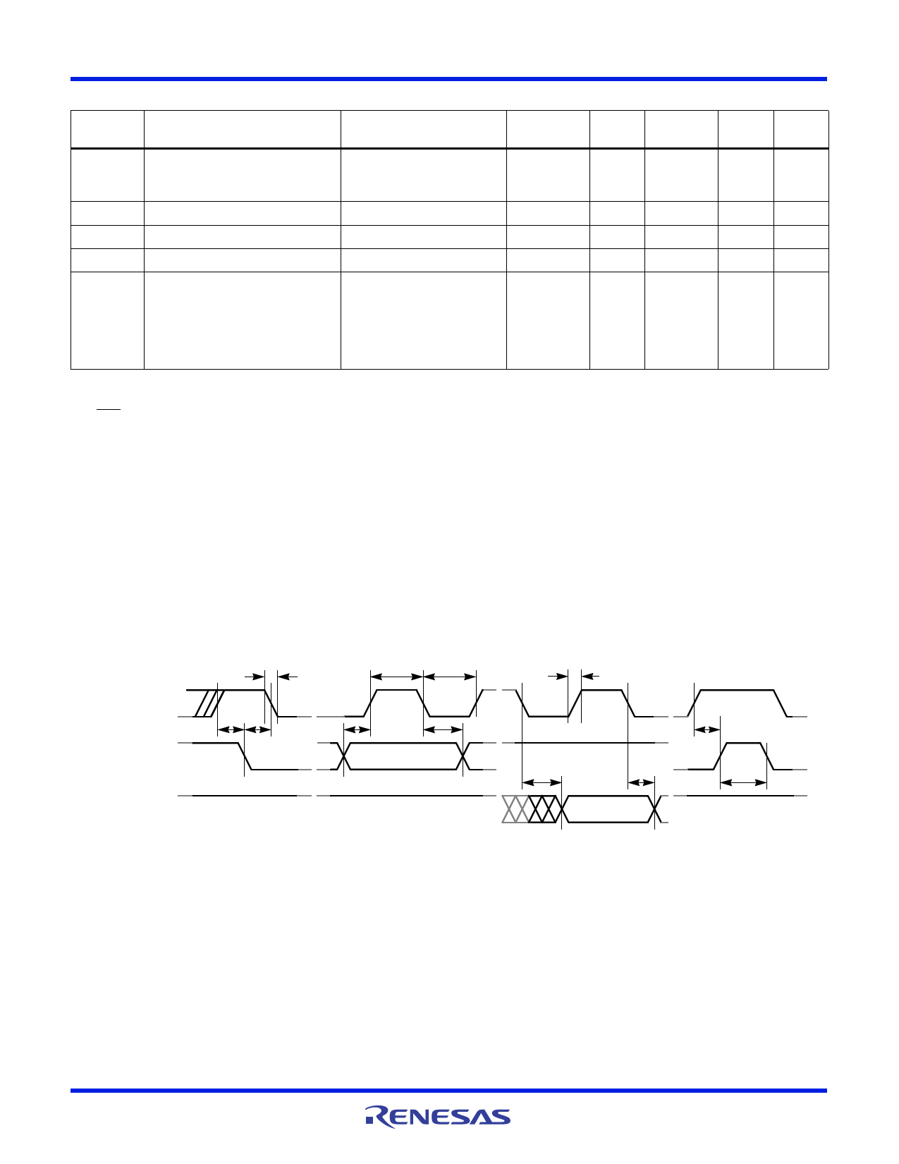
SDA vs SCL Timing
tF
tHIGH
tLOW
tR
SCL
tSU:STA
SDA
(INPUT TIMING)
SDA
(OUTPUT TIMING)
tSU:DAT
tHD:STA
tHD:DAT
tAA
tDH
tSU:STO
tBUF
FN6682 Rev 3.00
December 6, 2011
Page 5 of 29
Share Link: