ISL24021IRT065Z-T7A 데이터 시트보기 (PDF) - Renesas Electronics
부품명
상세내역
제조사
ISL24021IRT065Z-T7A Datasheet PDF : 13 Pages
| |||
ISL24021
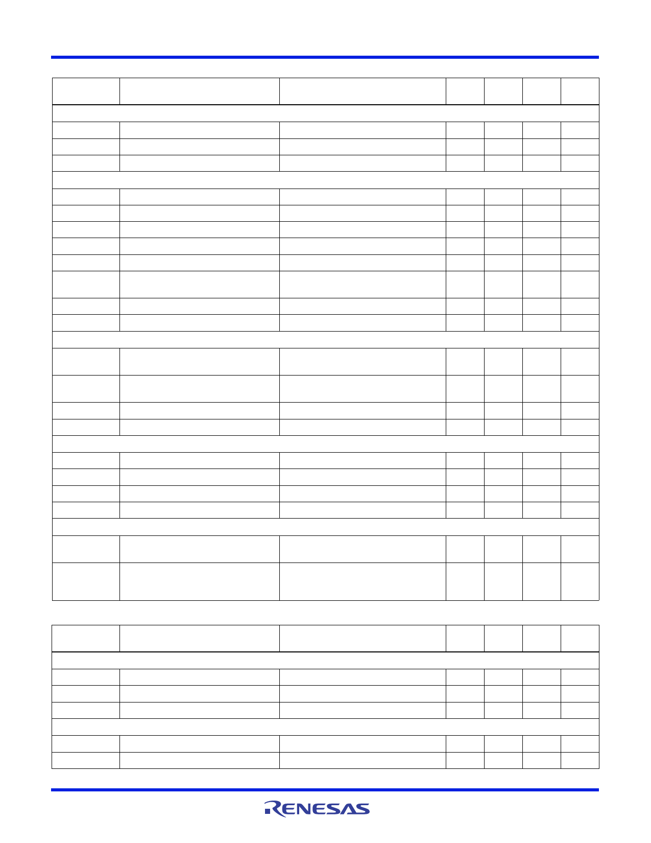
.Electrical Specifications VDD = 5V, VSS = GND = 0V, RL = 1kto 2.5V, TA = +25°C, Unless Otherwise Specified.
PARAMETER
DESCRIPTION
CONDITION
MIN
MAX
(Note 6) TYP (Note 6)
POWER SUPPLY PERFORMANCE
VDD - VSS
IS
PSRR
Supply Voltage Range
Supply Current
Power Supply Rejection Ratio
INPUT CHARACTERISTICS
No load
VS is moved from +4.5V to +19V
4.5
19
2.0
2.8
60
80
VOS
TCVOS
ILEAK
RIN
CIN
CMIR
Input Offset Voltage
Average Offset Voltage Drift (Note 7)
Input Leakage Current
Input Resistance
Input Capacitance
Common-Mode Input Range
VCM = 2.5V
VCM = 2.5V
1.4
15
1
2
10
1
2
VSS-
VDD+
0.5
0.5
CMRR
Common-Mode Rejection Ratio
AVOL
Open-Loop Gain
OUTPUT CHARACTERISTICS
For VIN from -0.5V to 5.5V
0.5V VOUT 4.5V
45
70
70
100
VOH
Output Swing High
IL= 5mA, VIN = VDD
VDD-
0.15
VDD-
0.025
VOL
Output Swing Low
IL= -5mA,VIN = VSS
VSS+
0.025
VSS+
0.15
ISC
Short-Circuit Current
IOUT
Continuous Output Current (Note 10)
DYNAMIC PERFORMANCE
±0.5
±300
SR
Slew Rate (Note 8)
1V VOUT 4V
15
tS
Settling to 0.1% (Note 9)
AV = +1, VO = 2V step
80
BW
-3dB Bandwidth
AV = +1, RL = 1kCL= 8pF
22
PM
Phase Margin
RL = 1kCL= 8pF
46
THERMAL PERFORMANCE
TTS
TTSH
Thermal Shutdown Temperature
Thermal Shutdown Hysteresis
Die temperature at which the device will
shutdown until it cools by TTSH °C
Die temperature below TTS °C when the
device will become operational after
shutdown
+165
15
UNIT
V
mA
dB
mV
µV/°C
nA
G
pF
V
dB
dB
V
V
A
mA
V/µs
ns
MHz
°
°C
°C
Electrical Specifications VDD = 15V, VSS = GND = 0V, RL = 1k to 7.5V, TA = +25°C, Unless Otherwise Specified.
PARAMETER
DESCRIPTION
CONDITION
MIN
MAX
(Note 6) TYP (Note 6) UNIT
POWER SUPPLY PERFORMANCE
VDD - VSS
IS
PSRR
Supply Voltage Range
Supply Current
Power Supply Rejection Ratio
INPUT CHARACTERISTICS
No load
VS is moved from +4.5V to +19V
4.5
19
V
2.2
2.8
mA
60
80
dB
VOS
TCVOS
Input Offset Voltage
Average Offset Voltage Drift (Note 7)
VCM = 7.5V
1.4
15
mV
1
µV/°C
FN6637 Rev 1.00
October 18, 2011
Page 3 of 13
Share Link: 