UPD16707A 데이터 시트보기 (PDF) - NEC => Renesas Technology
부품명
상세내역
제조사
UPD16707A Datasheet PDF : 13 Pages
| |||
µ PD16707A
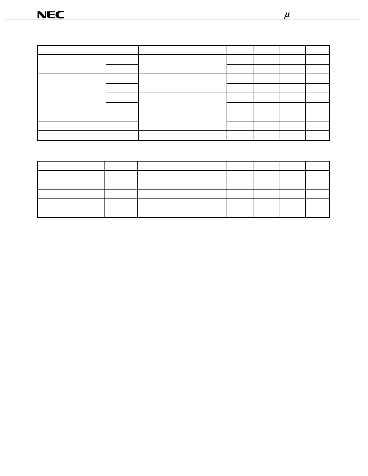
Switching Characteristics (TA = –20 to +75°C, VDD1 = 2.3 to 3.6 V, VDD2 = 20 V, VEE = –5 V, VSS = 0 V)
Parameter
★ Cascade Output Delay Time
Driver Output Delay Time
Output Rise Time
Output Fall Time
Input Capacitance
Symbol
tPHL1
tPLH1
tPHL2
tPLH2
tPHL3
tPLH3
tTLH
tTHL
CI
Condition
CL = 20 pF,
CLKR (CLKL) → STVL (STVR)
CL = 300 pF, CLKR (CLKL) → On
CL = 300 pF, OER (OEL) → On
CL = 300 pF
TA = 25°C
MIN.
TYP.
MAX.
Unit
500
ns
500
ns
500
ns
500
ns
500
ns
500
ns
800
ns
800
ns
15
pF
Timing Requirements (TA = −20 to +75°C, VDD1 = 2.3 to 3.6 V, VDD2 = 20 V, VEE = −5 V, VSS = 0 V)
Parameter
Symbol
Condition
MIN.
TYP.
MAX.
Unit
Clock Pulse High Width
PWCLK(H)
500
ns
Clock Pulse Low Width
PWCLK(L)
500
ns
Enable Pulse Width
PWOE
1000
ns
Data Setup Time
tSETUP
STVR (STVL) ↑→ CLKR, CLKL↑
200
ns
Data Hold Time
tHOLD
CLKR, CLKL ↑→ STVR (STVL) ↓
200
ns
Remark Unless otherwise specified, the input level is defined to be VIH = 0.8 VDD1, VIL = 0.2 VDD1.
Caution Keep the time and fall time of the logic input to tr = tf = 20 ns (10 to 90% of the rated values).
Data Sheet S16563EJ1V0DS
9
Share Link: 