L6229DP 데이터 시트보기 (PDF) - STMicroelectronics
부품명
상세내역
제조사
L6229DP Datasheet PDF : 33 Pages
| |||
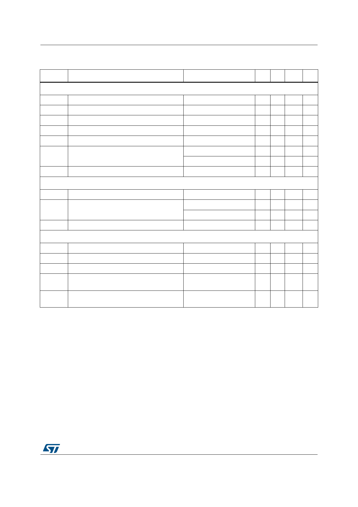
L6229
Electrical characteristics
Symbol
Table 6. Electrical characteristics
(VS = 48 V , Tamb = 25 °C , unless otherwise specified) (continued)
Parameter
Test conditions
Min. Typ. Max. Unit
PWM comparator and monostable
IRCOFF
VOFFSET
tprop
tblank
tON(min)
Source current at pin RCOFF
Offset voltage on sense comparator
Turn OFF propagation delay(3)
Internal blanking time on sense comparator
Minimum on time
tOFF PWM recirculation time
IBIAS Input bias current at pin VREF
TACHO monostable
VRCOFF = 2.5 V
Vref = 0.5 V
Vref = 0.5 V
-
3.5 5.5 - mA
- ±5 - mV
- 500 - ns
-1
- µs
-
- 2.5 3 µs
ROFF = 20 k; COFF 1 nF - 13
-
s
ROFF = 100 k; COFF 1 nF - 61
-
s
-
- - 10 µA
IRCPULSE Source current at pin RCPULSE
tPULSE Monostable of time
RTACHO Open drain ON resistance
VRCPULSE = 2.5 V
3.5 5.5 - mA
RPUL = 20 k; CPUL 1 nF - 12
-
s
RPUL = 100 k; CPUL 1 nF - 60
-
s
-
- 40 60
Overcurrent detection and protection
ISOVER
ROPDR
IOH
Supply overcurrent protection threshold
Open drain ON resistance
OCD high level leakage current
tOCD(ON) OCD turn-ON delay time(4)
tOCD(OFF) OCD turn-OFF delay time(9)
TJ = -25 to 125 °C(1)
IDIAG = 4 mA
VDIAG = 5 V
IDIAG = 4 mA;
CDIAG < 100 pF
IDIAG = 4 mA;
CDIAG < 100 pF
2 2.8 3.55 A
- 40 60
-1
- µA
- 200 - ns
- 100 - ns
1. Tested at 25 °C in a restricted range and guaranteed by characterization.
2. See Figure 3: Switching characteristic definition.
3. Measured applying a voltage of 1 V to pin SENSE and a voltage drop from 2 V to 0 V to pin VREF.
4. See Figure 4: Overcurrent detection timing definition.
DocID9455 Rev 5
9/33
33
Share Link: 