ISL59830A 데이터 시트보기 (PDF) - Renesas Electronics
부품명
상세내역
제조사
ISL59830A Datasheet PDF : 15 Pages
| |||
ISL59830A
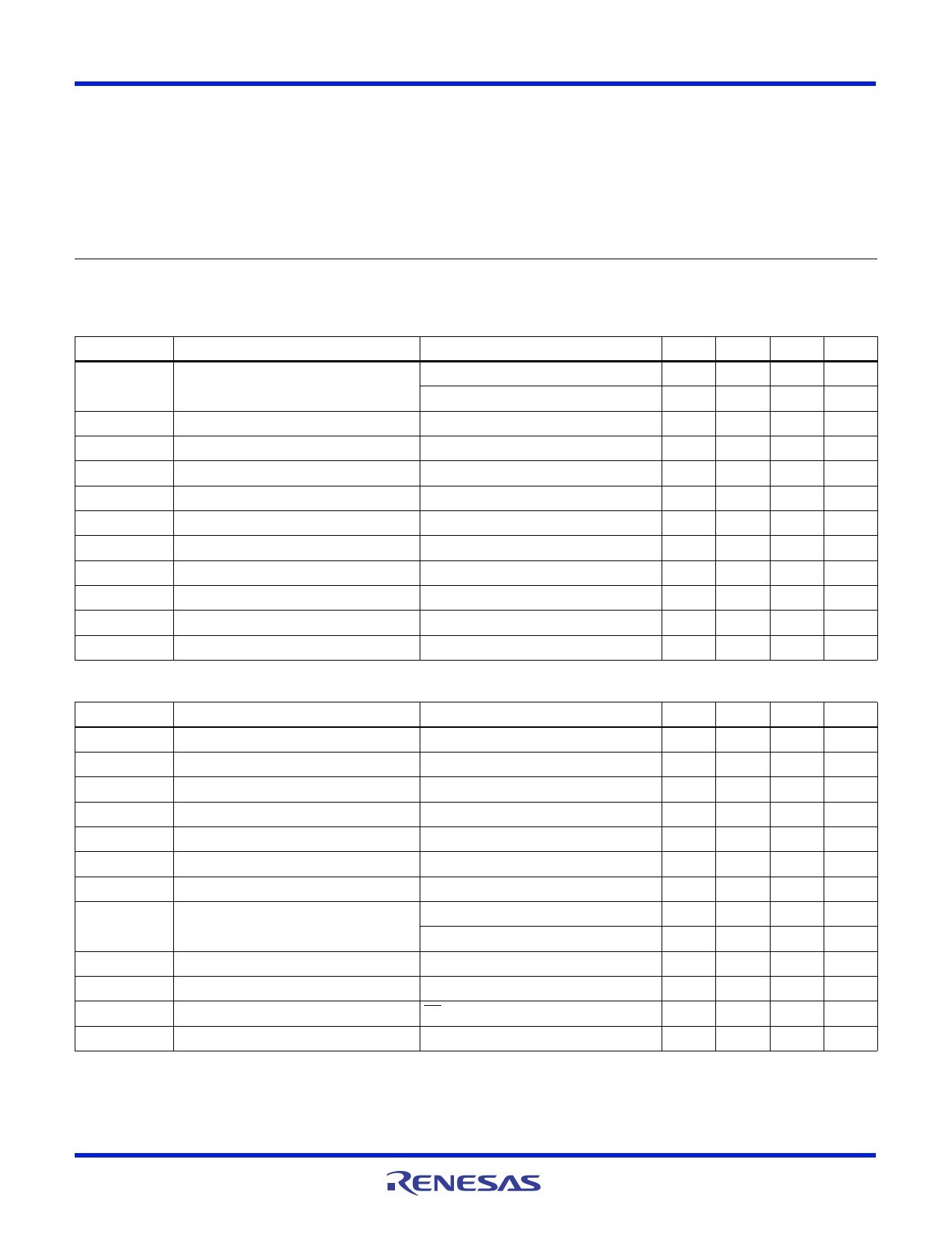
Absolute Maximum Ratings (TA = +25°C)
VCC, Supply Voltage between VS and GND5V
VIN, VREF . . . . . . . . . . . . . . . . . . . . . . . . . . . .VCC+0.3V, VEE-0.3V
Voltage between VIN and VREF. . . . . . . . . . . . . . . . . . . . . . . . . .±2V
Maximum Continuous Output Current . . . . . . . . . . . . . . . . . . . 30mA
Operating Temperature . . . . . . . . . . . . . . . . . . . . . . .-40°C to +85°C
Maximum Die Temperature . . . . . . . . . . . . . . . . . . . . . . . . . . +150°C
Storage Temperature . . . . . . . . . . . . . . . . . . . . . . . .-65°C to +150°C
Lead Temperature . . . . . . . . . . . . . . . . . . . . . . . . . . . . . . . . . +260°C
Power Dissipation . . . . . . . . . . . . . . . . . . . . . . . . . . . . . See Curves
CAUTION: Stresses above those listed in “Absolute Maximum Ratings” may cause permanent damage to the device. This is a stress only rating and operation of the
device at these or any other conditions above those indicated in the operational sections of this specification is not implied.
IMPORTANT NOTE: All parameters having Min/Max specifications are guaranteed. Typical values are for information purposes only. Unless otherwise noted, all tests
are at the specified temperature and are pulsed tests, therefore: TJ = TC = TA
AC Electrical Specifications VCC = DVCC = +3.3V, REF = GND, TA = +25°C, RL = 150, unless otherwise specified.
PARAMETER
DESCRIPTION
CONDITIONS
MIN TYP MAX
BW -3dB
BW 0.1dB
SR
dG
dP
XT
I
3dB Bandwidth
0.1dB Bandwidth
Slew Rate
Differential Gain
Differential Phase
Hostile Crosstalk
Input to Output Isolation
VOUT = 200mVPP
VOUT = 2VPP
VOUT = 2VPP
VOUT = 2VPP
6MHz
6MHz
200
100
50
500
.06
0.1
-90
-70
VN
Input Noise Voltage
20
CSW Freq
Charge Pump Switch Frequency
168
Load Reg
VRIPPLE
Ripple Voltage
IEE = 0mA to 10mA
12
60
30
UNIT
MHz
MHz
MHz
V/µs
%
°
dB
dB
nV/Hz
MHz
mV
mV
DC Electrical Specifications VCC = DVCC = +3.3V, REF = GND, TA = +25°C, RL = 150, unless otherwise specified.
PARAMETER
DESCRIPTION
CONDITIONS
MIN TYP MAX
V+
Supply Range
3.0
3.6
VG%
GM
RIN
VOS
IOUT +
IOUT -
ZOUT
Gain Error
Gain Matching
Input Resistance
Output Offset Voltage
Output Current
Output Current
Output Impedance
RL = 150, VIN = +2.5V to -1V
RL = 150
VIN = 0V to 1.5V
VREF = 0
RL = 10, VIN = 1.2V
RL = 10, VIN = -0.3V
Enabled
Three-stated
1.5
0.5
1.0
1.7
15
-25
7
+25
50
-18
1
10
PSRR
Power Supply Rejection Ratio
60
90
IS
IS_PD
RREF
Supply Current
Power Down Supply Current
Input Reference Resistor
Enabled
EN = PD = 3.3V
150
0.9
4
5
6
UNIT
V
%
%
M
mV
mA
mA
M
dB
mA
mA
k
FN6233 Rev.3.00
Sep 26, 2006
Page 2 of 15
Share Link: 