MB90372PMT-G-XXX 데이터 시트보기 (PDF) - Fujitsu
부품명
상세내역
제조사
MB90372PMT-G-XXX Datasheet PDF : 153 Pages
| |||
MB90370 Series
(Continued)
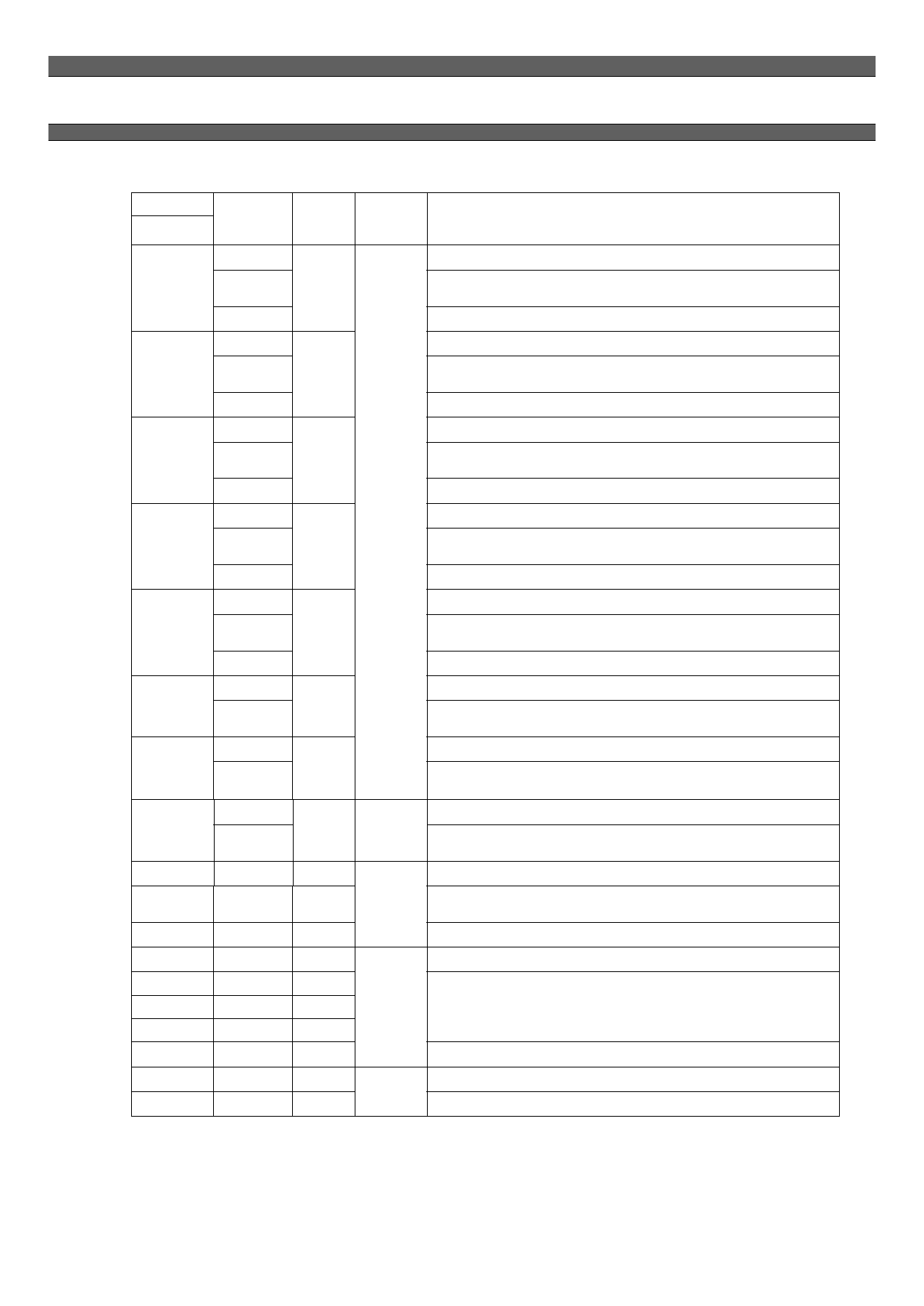
Pin no.
LQFP-144
Pin name
Pin status
I/O circuit during
reset
Function
PE3
General-purpose I/O port.
77
SEG3
O
TO2
PE4
Segment output pin for LCD controller/driver. This function is selected when LCD
segment output is enabled.
Event output pin for reload timer 2.
General-purpose I/O port.
78
SEG4
O
TIN3
PE5
Segment output pin for LCD controller/driver. This function is selected when LCD
segment output is enabled.
External clock input pin for reload timer 3.
General-purpose I/O port.
79
SEG5
O
Segment output pin for LCD controller/driver. This function is selected when LCD
segment output is enabled.
TO3
Event output pin for reload timer 3.
PE6
Port input General-purpose I/O port.
80
SEG6
O
Segment output pin for LCD controller/driver. This function is selected when LCD
segment output is enabled.
TIN4
External clock input pin for reload timer 4.
PE7
General-purpose I/O port.
81
SEG7
O
TO4
PF0
82
P
SEG8
PF1 ~ PF4
83 ~ 86
COM0 ~
P
COM3
Segment output pin for LCD controller/driver. This function is selected when LCD
segment output is enabled.
Event output pin for reload timer 4.
General-purpose I/O port.
Segment output pin for LCD controller/driver. This function is selected when LCD
segment output is enabled.
General-purpose I/O port.
COM output pin for LCD controller/driver. This function is selected when LCD COM
output is enabled.
PF5 ~ PF7
87 ~ 89
Q
V1 ~ V3
42
AVCC
R
43
AVR
S
Power
input
Power
input
General-purpose I/O port.
Power input pin for LCD controller/driver. This function is selected when external
voltage divider is enabled.
Vcc power input pin for analog circuits.
Vref+ input pin for the A/D converter. This voltage must not exceed Vcc. Vref- is
fixed to AVSS.
44
AVSS
R
Vss power input pin for analog circuits.
29
CVCC
R
Vcc power input pin for analog circuits.
30
CVRH1
R
Power
31
CVRH2
R
input Standard power input pin of the comparator.
32
CVRL
R
33
19,55,91,127
18,54,90,126
CVSS
Vss
Vcc
R
Vss power input pin for analog circuits.
–
Power Power (0 V) input pin.
–
input
Power (3.3 V) input pin.
10
Share Link: 