ISL80136 데이터 시트보기 (PDF) - Renesas Electronics
부품명
상세내역
제조사
ISL80136 Datasheet PDF : 10 Pages
| |||
ISL80136
Absolute Maximum Ratings
IN Pin to GND Voltage . . . . . . . . . . . . . . . . . . . . . . . . . . . GND - 0.3V to +45V
OUT Pin to GND Voltage . . . . . . . . . . . . . . . . . . . . . . . . . . . GND - 0.3V to 16V
EN Pin to GND Voltage . . . . . . . . . . . . . . . . . . . . . . . . . . . . . .GND - 0.3V to IN
ADJ Pin to GND Voltage . . . . . . . . . . . . . . . . . . . . . . . . . . . . . GND - 0.3V to3V
Output Short-circuit Duration . . . . . . . . . . . . . . . . . . . . . . . . . . . . . Indefinite
ESD Rating
Human Body Model (Tested per JESD22-A114E) . . . . . . . . . . . . . . . . 5kV
Machine Model (Tested per JESD-A115-A) . . . . . . . . . . . . . . . . . . . 200V
Charge Device Model (Tested per JESD22-C101C). . . . . . . . . . . . . 2.2kV
Latch-up (Tested per JESD78B; Class II, Level A) . . . . . . . . . . . . . . . 100mA
Thermal Information
Thermal Resistance (Typical)
JA (°C/W) JC (°C/W)
8 Ld EPSOIC Package (Notes 4, 5). . . . . . . .
50
9
Maximum Junction Temperature . . . . . . . . . . . . . . . . . . . . . . . . . . . +150°C
Maximum Storage Temperature Range . . . . . . . . . . . . . .-65°C to +175°C
Pb-free Reflow Profile . . . . . . . . . . . . . . . . . . . . . . . . . . . . . . . . . . see TB493
Recommended Operating Conditions
Ambient Temperature Range . . . . . . . . . . . . . . . . . . . . . . -40°C to +125°C
IN Pin to GND Voltage . . . . . . . . . . . . . . . . . . . . . . . . . . . . . . . . . +6V to +40V
OUT Pin to GND Voltage . . . . . . . . . . . . . . . . . . . . . . . . . . . . . +2.5V to +12V
EN Pin to GND Voltage . . . . . . . . . . . . . . . . . . . . . . . . . . . . . . . . . . 0V to +40V
CAUTION: Do not operate at or near the maximum ratings listed for extended periods of time. Exposure to such conditions may adversely impact product
reliability and result in failures not covered by warranty.
NOTES:
4. JA is measured in free air with the component mounted on a high effective thermal conductivity test board with “direct attach” features. See Tech
Brief TB379.
5. For JC, the “case temp” location is the center of the exposed metal pad on the package underside.
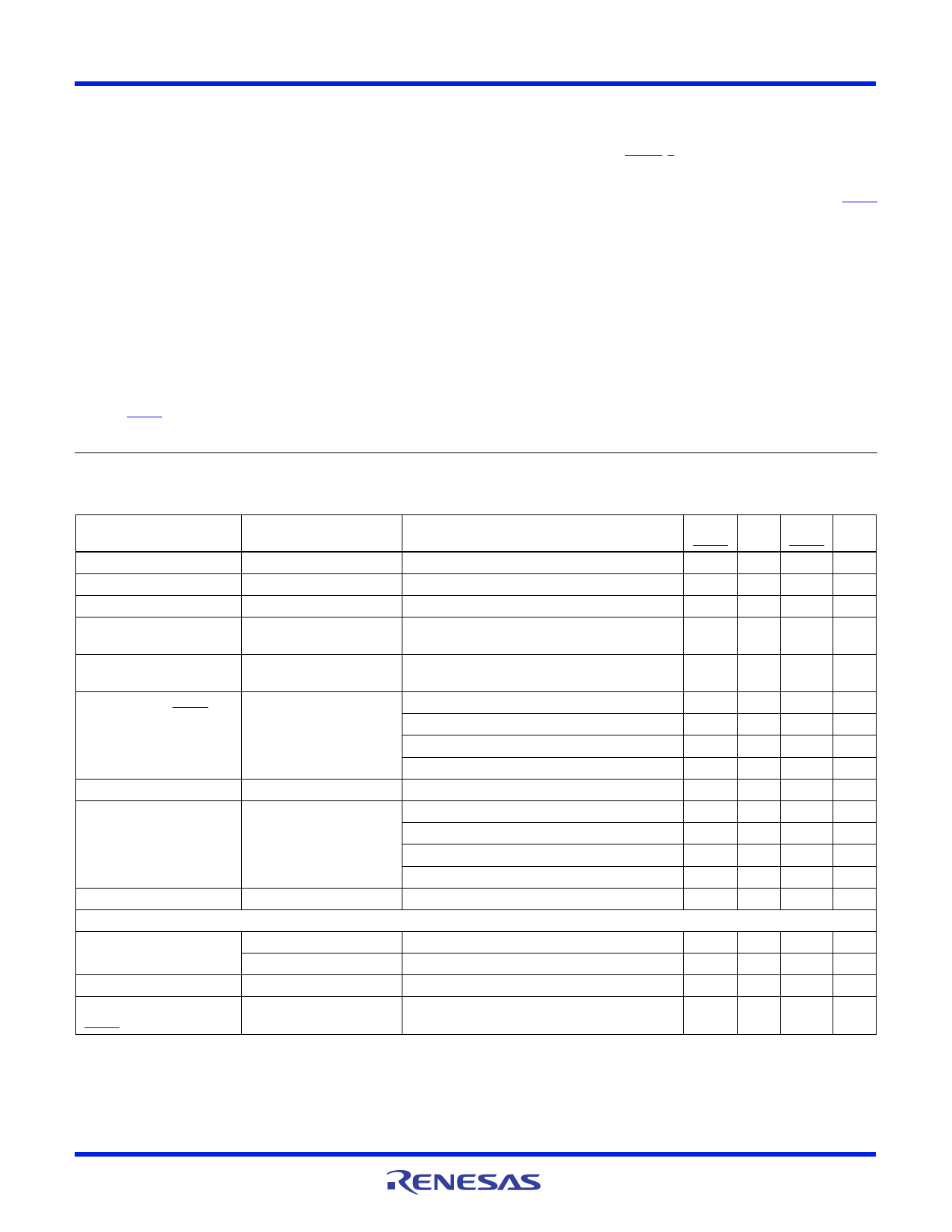
Electrical Specifications Recommended Operating Conditions, unless otherwise noted. VIN = 14V, IOUT = 1mA, TA = TJ = -40°C to
+125°C, unless otherwise noted. Typical specifications are at TA = +25°C. Boldface limits apply across the operating temperature range, -40°C to
+125°C.
PARAMETER
SYMBOL
TEST CONDITIONS
MIN
MAX
(Note 8) TYP (Note 8) UNITS
Input Voltage Range
VIN
6
40
V
Guaranteed Output Current
IOUT
VIN = VOUT + VDO
50
mA
ADJ Reference Voltage
VREF
EN = High, VIN = 14V, IOUT = 0.1mA to 50mA
1.211 1.223 1.235 V
Line Regulation
(VOUT low line - VOUT high 6V < VIN < 40V, IOUT = 1mA
line)/VOUT low line
0.04 0.115 %
Load Regulation
(VOUT no load - VOUT high VIN = 14V, IOUT = 100µA to 50mA
load)/VOUT no load
0.25 0.5
%
Dropout Voltage (Note 6)
VDO
IOUT = 1mA, VOUT = 2.5V
10
38
mV
IOUT = 50mA, VOUT = 2.5V
130 340 mV
IOUT = 1mA, VOUT = 5V
10
48
mV
IOUT = 50mA, VOUT = 5V
120 350 mV
Shutdown Current
ISHDN
EN = LOW
1.8 3.64 µA
Quiescent Current
IQ
EN = HIGH, IOUT = 0mA
18
24
µA
EN = HIGH, IOUT = 1mA
22
42
µA
EN = HIGH, IOUT = 10mA
34
60
µA
EN = HIGH, IOUT = 50mA
56
82
µA
Power Supply Rejection Ratio
PSRR
f = 100Hz; VIN_RIPPLE = 500mVP-P; Load = 50mA
58
dB
EN FUNCTION
EN Threshold Voltage
EN Pin Current
EN to Regulation Time
(Note 7)
VEN_H
VEN_L
IEN
tEN
VOUT = Off to On
VOUT = On to Off
VOUT = 0V
1.485 V
0.935
V
0.026
µA
1.65 1.93 ms
FN7970 Rev 2.00
August 11, 2015
Page 4 of 10
Share Link: 