ISL8840AABZ 데이터 시트보기 (PDF) - Renesas Electronics
부품명
상세내역
제조사
ISL8840AABZ
Renesas Electronics

ISL8840AABZ Datasheet PDF : 15 Pages
| |||
ISL8840A, ISL8841A, ISL8842A, ISL8843A, ISL8844A, ISL8845A
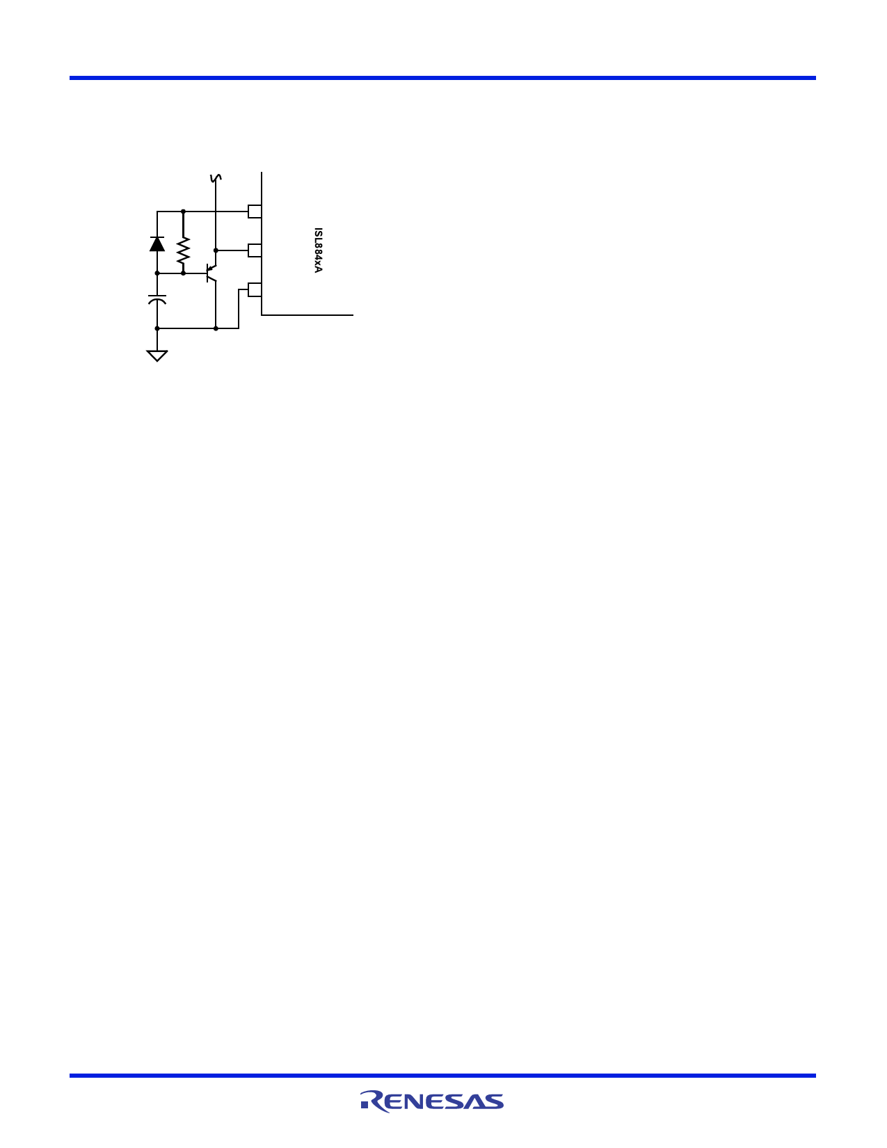
Soft-Start Operation
Soft-start must be implemented externally. One method,
illustrated below, clamps the voltage on COMP.
From the small signal current-mode model [1] it can be shown
that the naturally-sampled modulator gain, Fm, without slope
compensation, is in Equation 6.
Fm = S-----n----T1----s---w---
(EQ. 6)
VREF
D1
R1
COMP
Q1
GND
C1
FIGURE 5. SOFT-START
The COMP pin is clamped to the voltage on capacitor C1 plus
a base-emitter junction by transistor Q1. C1 is charged from
VREF through resistor R1 and the base current of Q1. At
power-up C1 is fully discharged, COMP is at ~0.7V, and the
duty cycle is zero. As C1 charges, the voltage on COMP
increases, and the duty cycle increases in proportion to the
voltage on C1. When COMP reaches the steady state
operating point, the control loop takes over and soft start is
complete. C1 continues to charge up to VREF and no longer
affects COMP. During power down, diode D1 quickly
discharges C1 so that the soft start circuit is properly initialized
prior to the next power on sequence.
Gate Drive
The ISL884xA is capable of sourcing and sinking 1A peak
current. To limit the peak current through the IC, an optional
external resistor may be placed between the totem-pole output
of the IC (OUT pin) and the gate of the MOSFET. This small
series resistor also damps any oscillations caused by the
resonant tank of the parasitic inductances in the traces of the
board and the FET’s input capacitance.
Slope Compensation
For applications where the maximum duty cycle is less than
50%, slope compensation may be used to improve noise
immunity, particularly at lighter loads. The amount of slope
compensation required for noise immunity is determined
empirically, but is generally about 10% of the full scale current
feedback signal. For applications where the duty cycle is
greater than 50%, slope compensation is required to prevent
instability.
Slope compensation may be accomplished by summing an
external ramp with the current feedback signal or by
subtracting the external ramp from the voltage feedback error
signal. Adding the external ramp to the current feedback signal
is the more popular method.
where Sn is the slope of the sawtooth signal and Tsw is the
duration of the half-cycle. When an external ramp is added, the
modulator gain becomes:
Fm = ---S----n-----+-----S-1----e------T----s---w--- = -m-----c---S----1n----T----s----w--
(EQ. 7)
where Se is slope of the external ramp and
mc = 1 + SS-----en--
(EQ. 8)
The criteria for determining the correct amount of external
ramp can be determined by appropriately setting the damping
factor of the double-pole located at the switching frequency.
The double-pole will be critically damped if the Q-factor is set
to 1, over-damped for Q < 1, and under-damped for Q > 1. An
under-damped condition may result in current loop instability.
Q = -------m-----c-----1-----–--1---D--------–-----0---.--5----
(EQ. 9)
where D is the percent of on time during a switching cycle.
Setting Q = 1 and solving for Se yields
Se
=
Sn
1--
+
0.5
1-----–-1----D---
–
1
(EQ. 10)
Since Sn and Se are the on time slopes of the current ramp
and the external ramp, respectively, they can be multiplied by
tON to obtain the voltage change that occurs during tON.
Ve
=
Vn
1--
+
0.5
1-----–-1----D---
–
1
(EQ. 11)
where Vn is the change in the current feedback signal (I)
during the on time and Ve is the voltage that must be added by
the external ramp.
For a flyback converter, Vn can be solved for in terms of input
voltage, current transducer components, and primary
inductance, yielding
Ve
=
D---------T----S----W-------L---Vp----I--N--------R-----C----S--
1--
+
0.5
1-----–-1----D---
–
1
V
(EQ. 12)
where RCS is the current sense resistor, fsw is the switching
frequency, Lp is the primary inductance, VIN is the minimum
input voltage, and D is the maximum duty cycle.
FN6320 Rev 3.00
April 18, 2007
Page 11 of 15
Share Link: