CAV24C64C4CTR(2016) 데이터 시트보기 (PDF) - ON Semiconductor
부품명
상세내역
제조사
CAV24C64C4CTR Datasheet PDF : 11 Pages
| |||
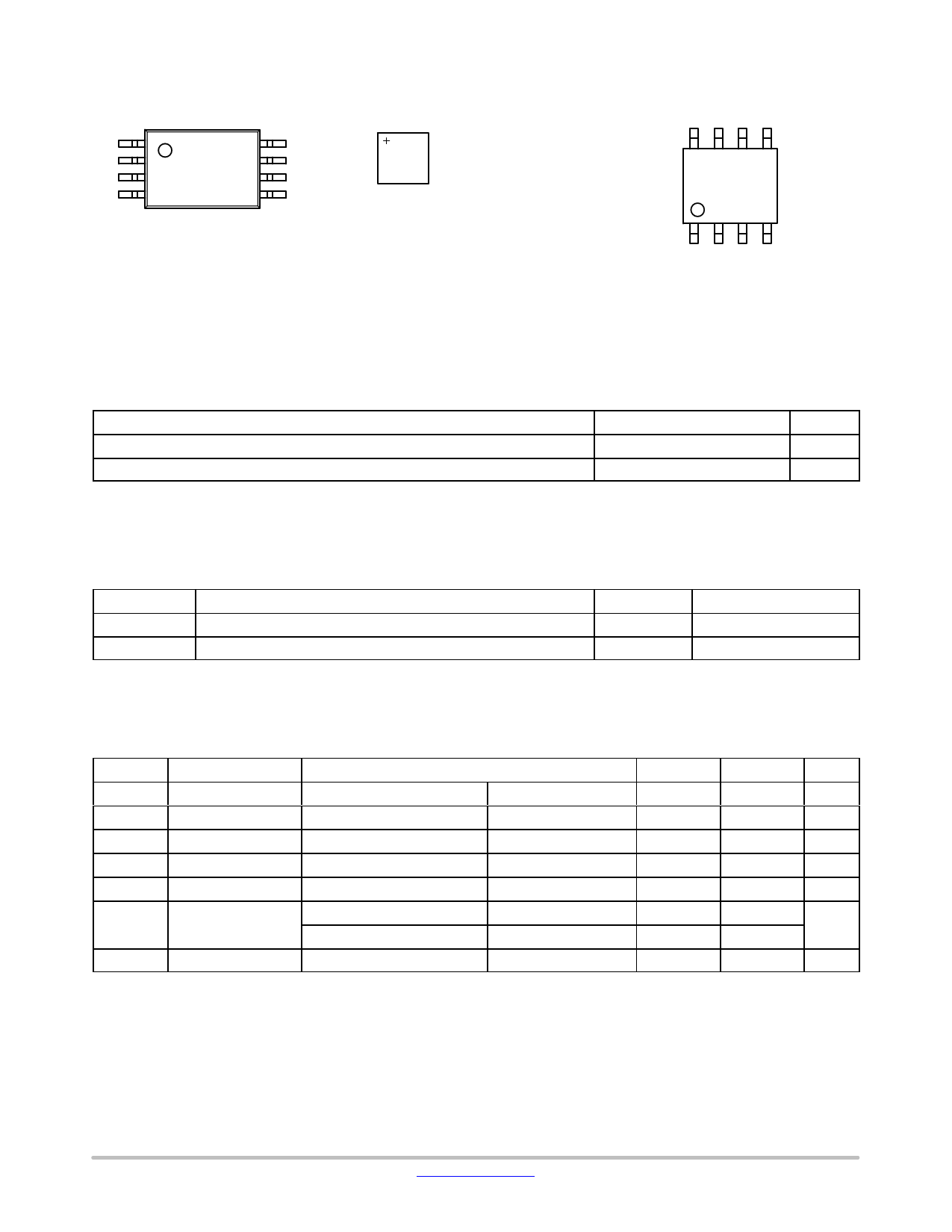
CAV24C64
(TSSOP−8)
DEVICE MARKINGS
(WLCSP−4)
(SOIC−8)
C64F
A
Y
M
XXX
G
C64F
AYMXXX
G
A For the location of Pin 1,
YM please consult the corre-
sponding package drawing.
A = Specific Device Code
24C64F
AYMXXX
G
= Specific Device Code
= Assembly Location
Y = Production Year (Last Digit)
M = Production Month (1−9, O, N, D)
= Production Year (Last Digit)
= Production Month (1-9, O, N, D)
= Last Three Digits of Assembly Lot Number
= Pb−Free Package
24C64F = Specific Device Code
A
= Assembly Location
Y
= Production Year (Last Digit)
M
= Production Month (1-9, O, N, D)
XXX = Last Three Digits of Assembly Lot Number
G
= Pb−Free Package
Table 1. ABSOLUTE MAXIMUM RATINGS
Parameters
Ratings
Units
Storage Temperature
–65 to +150
°C
Voltage on Any Pin with Respect to Ground (Note 1)
–0.5 to +6.5
V
Stresses exceeding those listed in the Maximum Ratings table may damage the device. If any of these limits are exceeded, device functionality
should not be assumed, damage may occur and reliability may be affected.
1. During input transitions, voltage undershoot on any pin should not exceed −1 V for more than 20 ns. Voltage overshoot on pins A0, A1, A2
and WP should not exceed VCC + 1 V for more than 20 ns, while voltage on the I2C bus pins, SCL and SDA, should not exceed the absolute
maximum ratings, irrespective of VCC.
Table 2. RELIABILITY CHARACTERISTICS (Note 2)
Symbol
Parameter
Min
Units
NEND (Note 3) Endurance
1,000,000
Program/Erase Cycles
TDR
Data Retention
100
Years
2. These parameters are tested initially and after a design or process change that affects the parameter according to appropriate AEC−Q100
and JEDEC test methods.
3. Page Mode, VCC = 5 V, 25°C.
Table 3. D.C. OPERATING CHARACTERISTICS (VCC = 2.5 V to 5.5 V, TA = −40°C to +125°C, unless otherwise specified.)
Symbol
Parameter
Test Conditions
Min
Max
Units
ICCR
Read Current
Read, fSCL = 400 kHz
1
mA
ICCW
Write Current
Write, fSCL = 400 kHz
2
mA
ISB
Standby Current
All I/O Pins at GND or VCC
TA = −40°C to +125°C
5
mA
IL
I/O Pin Leakage
Pin at GND or VCC
2
mA
VIL
Input Low Voltage
−0.5
0.3 x VCC
V
VIH
Input High Voltage
A0, A1, A2 and WP
0.7 x VCC
VCC + 0.5
V
SCL and SDA
0.7 x VCC
5.5
VOL
Output Low Voltage
VCC > 2.5 V, IOL = 3 mA
0.4
V
Product parametric performance is indicated in the Electrical Characteristics for the listed test conditions, unless otherwise noted. Product
performance may not be indicated by the Electrical Characteristics if operated under different conditions.
www.onsemi.com
2
Share Link: 