74LVC07A 데이터 시트보기 (PDF) - Nexperia B.V. All rights reserved
부품명
상세내역
제조사
74LVC07A Datasheet PDF : 12 Pages
| |||
Nexperia
4. Functional diagram
74LVC07A
Hex buffer with open-drain outputs
1 1A
1Y 2
3 2A
2Y 4
5 3A
3Y 6
9 4A
4Y 8
11 5A
5Y 10
13 6A
6Y 12
mna535
Fig. 1. Logic symbol
1A 1
1
2 1Y
2A 3
1
4 2Y
3A 5
1
6 3Y
9
4A
1
8 4Y
11
1
5A
10
5Y
13
1
6A
12 6Y
mna534
Fig. 2. IEC logic symbol
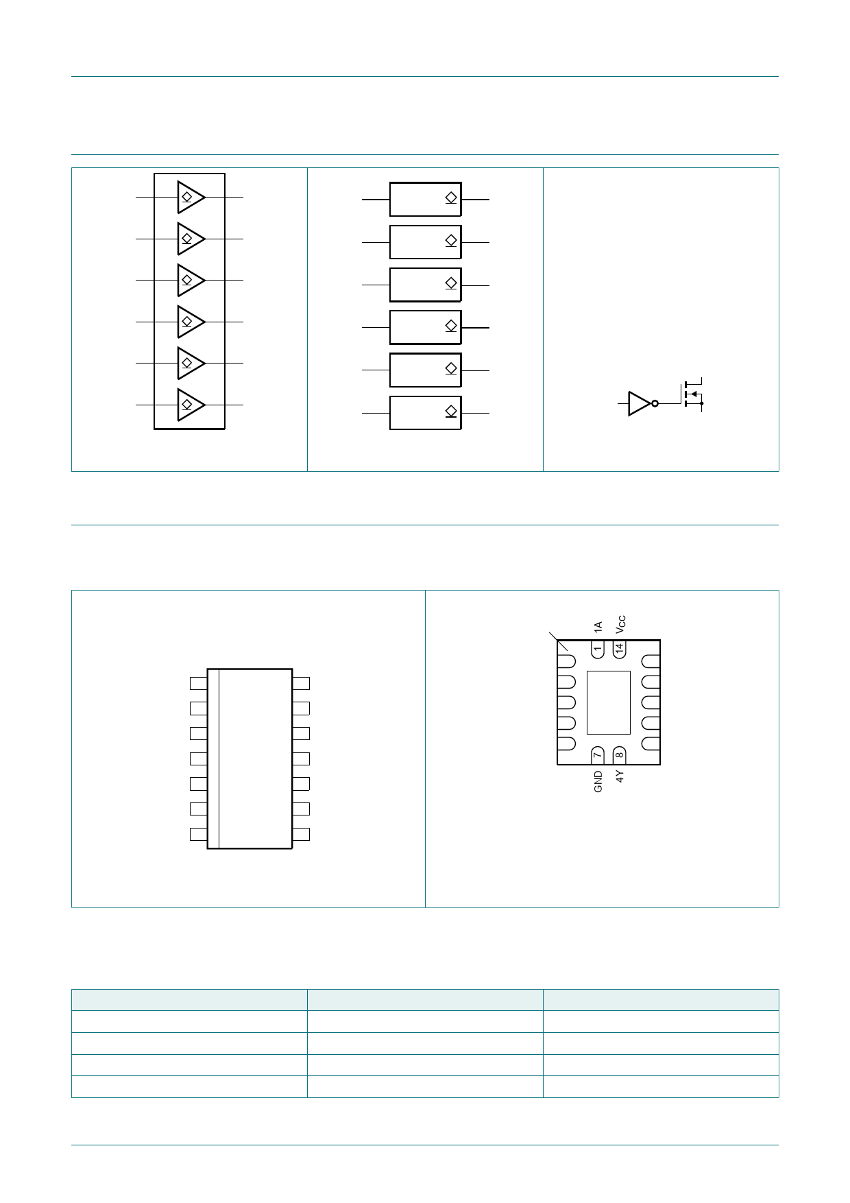
5. Pinning information
Y
A
GND
mna533
Fig. 3. Logic diagram for one gate
5.1. Pinning
74LVC07A
1A 1
1Y 2
14 VCC
13 6A
2A 3
12 6Y
2Y 4
11 5A
3A 5
10 5Y
3Y 6
9 4A
GND 7
8 4Y
001aad066
Fig. 4. Pin configuration for SOT108-1 (SO14) and
SOT402-1 (TSSOP14)
74LVC07A
terminal 1
index area
1Y 2
2A 3
2Y 4
3A 5
3Y 6
GND(1)
13 6A
12 6Y
11 5A
10 5Y
9 4A
001aad067
Transparent top view
(1) This is not a ground pin. There is no electrical or
mechanical requirement to solder the pad. In case
soldered, the solder land should remain floating or
connected to GND.
Fig. 5. Pin configuration for SOT762-1 (DHVQFN14)
5.2. Pin description
Table 2. Pin description
Symbol
1A, 2A, 3A, 4A, 5A, 6A
1Y, 2Y, 3Y, 4Y, 5Y, 6Y
GND
VCC
Pin
1, 3, 5, 9, 11, 13
2, 4, 6, 8, 10, 12
7
14
Description
data input
data output
ground (0 V)
supply voltage
74LVC07A
Product data sheet
All information provided in this document is subject to legal disclaimers.
Rev. 7 — 3 August 2020
© Nexperia B.V. 2020. All rights reserved
2 / 12
Share Link: 