74LVC07A 데이터 시트보기 (PDF) - Nexperia B.V. All rights reserved
부품명
상세내역
제조사
74LVC07A Datasheet PDF : 12 Pages
| |||
Nexperia
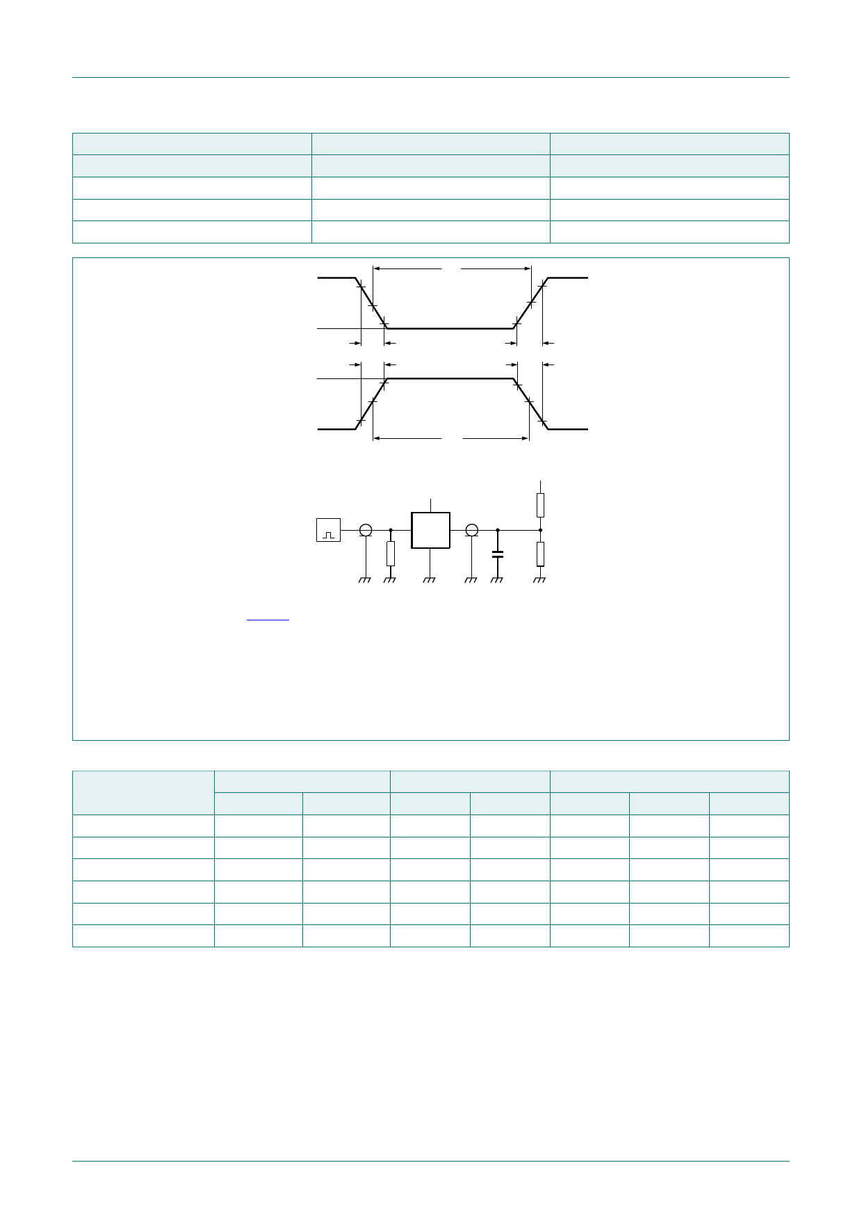
Table 8. Measurement points
Supply voltage
VCC
< 2.7 V
≥ 2.7 V to 3.6 V
≥ 4.5 V to 5.5 V
Input
VM
0.5 × VCC
1.5 V
0.5 × VCC
74LVC07A
Hex buffer with open-drain outputs
Output
VX
VOL + 0.15 V
VOL + 0.3 V
VOL + 0.3 V
VI 90 %
tW
negative
pulse
VM
10 %
0V
tf
VI
positive
pulse
tr
90 %
VM
10 %
0V
tW
VM
tr
tf
VM
VI
G
VCC
VO
DUT
VEXT
RL
RT
CL
RL
Fig. 7.
001aae331
Test data is given in Table 9.
Definitions for test circuit:
RL = Load resistance.
CL = Load capacitance including jig and probe capacitance.
RT = Termination resistance should be equal to output impedance Zo of the pulse generator.
VEXT = External voltage for measuring switching times.
Test circuit for measuring switching times
Table 9. Test data
Supply voltage
1.2 V
1.65 V to 1.95 V
2.3 V to 2.7 V
2.7 V
3.0 V to 3.6 V
4.5 V to 5.5 V
Input
VI
VCC
VCC
VCC
2.7 V
2.7 V
VCC
tr, tf
≤ 2 ns
≤ 2 ns
≤ 2 ns
≤ 2.5 ns
≤ 2.5 ns
≤ 2.5 ns
Load
CL
30 pF
30 pF
30 pF
50 pF
50 pF
50 pF
RL
1 kΩ
1 kΩ
500 Ω
500 Ω
500 Ω
500 Ω
VEXT
tPLH, tPHL
open
open
open
open
open
open
tPLZ, tPZL
2 × VCC
2 × VCC
2 × VCC
2 × VCC
2 × VCC
2 × VCC
tPHZ, tPZH
GND
GND
GND
GND
GND
GND
74LVC07A
Product data sheet
All information provided in this document is subject to legal disclaimers.
Rev. 7 — 3 August 2020
© Nexperia B.V. 2020. All rights reserved
6 / 12
Share Link: 