LT1635CN8(RevA) 데이터 시트보기 (PDF) - Linear Technology
부품명
상세내역
제조사
LT1635CN8 Datasheet PDF : 12 Pages
| |||
LT1635
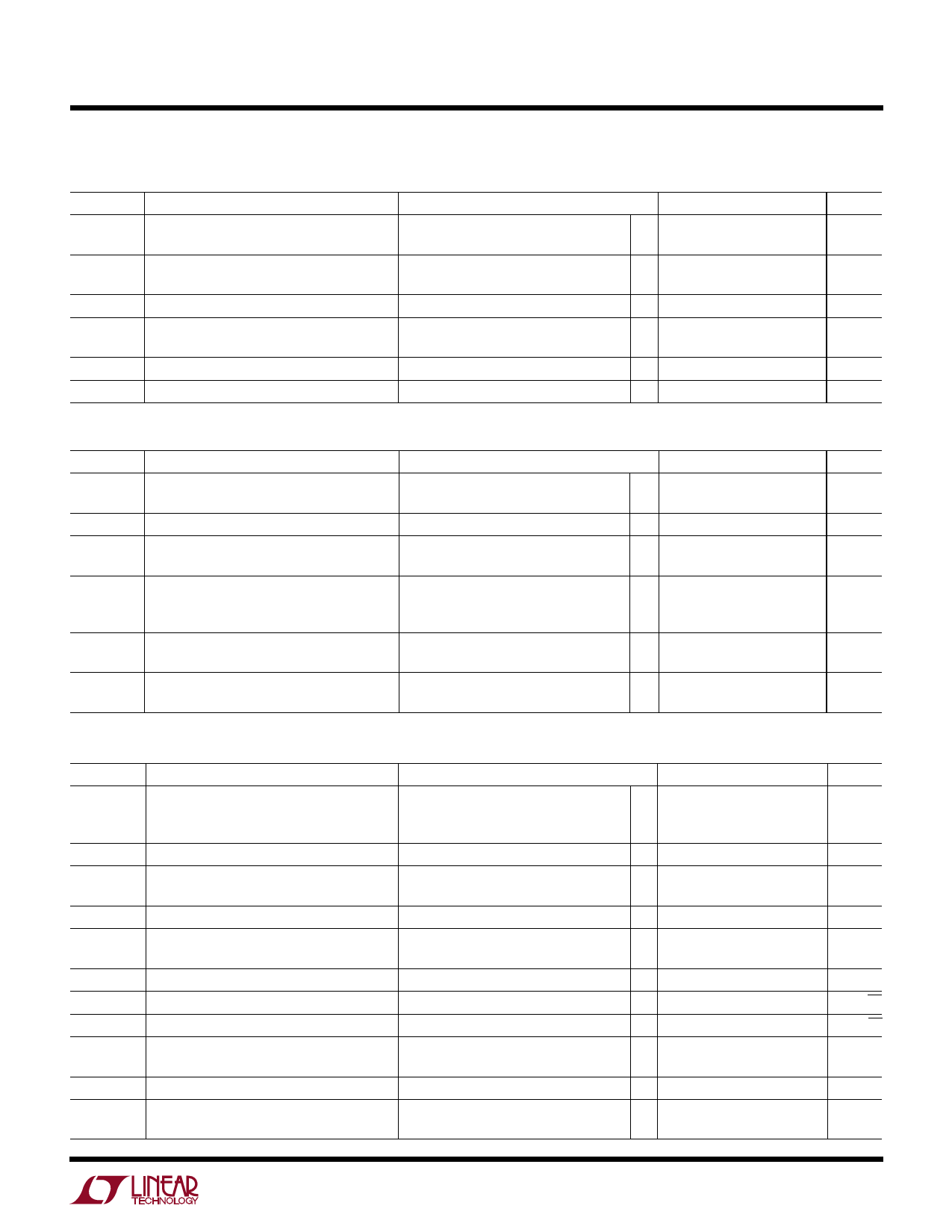
ELECTRICAL CHARACTERISTICS
5V OP AMP: The q denotes the specifications which apply over the full operating temperature range, otherwise specifications are at
TA = 25°C. VS = 5V, 0V; VCM = VOUT = 2.5V, unless otherwise noted. (Note 2)
SYMBOL
PARAMETER
CONDITIONS
MIN TYP MAX
UNITS
ISC
Short-Circuit Current
VS = 5V, Short to GND
q 20
40
mA
VS = 5V, Short to VCC
q 20
40
mA
PSRR
Power Supply Rejection Ratio
VS = 1.2V to 12V, VCM = VO = 0.2V
93
100
dB
q 90
97
dB
Minimum Operating Supply Voltage
(Note 3)
q
1.1
1.2
V
IS
Supply Current
130 200
µA
q
150 260
µA
GBW
Gain Bandwidth Product
f = 1kHz
175
kHz
SR
Slew Rate
AV = – 1, RL = ∞
0.045
V/µs
5V REFERENCE: The q denotes the specifications which apply over the full operating temperature range, otherwise specifications
are at TA = 25°C. VS = 5V, 0V, unless otherwise noted. (Note 2)
SYMBOL
PARAMETER
CONDITIONS
MIN TYP MAX
UNITS
VREF
Feedback Sense Voltage
Voltage at Pin 1 with Pin 1 Connected
q 189
200
211
mV
to Pin 8 (Note 6)
TC VREF
Reference Drift
Feedback Current
(Note 4)
Current into Pin 8
q
30
100 ppm/°C
3.5
10
nA
q
5.0
15
nA
Line Regulation
Load Regulation
0 ≤ IREF ≤ 1mA, VREF = 200mV
VS = 1.2V to 5V
VS = 1.3V to 5V (Note 3)
q
IREF = 0 to 1mA
q
20
100
ppm / V
30
200
ppm / V
150 300 ppm/mA
200 500 ppm/mA
Reference Amplifier Gain
VO = 0.2V to 3.5V
45
90
q 25
50
V/mV
V/mV
±5V OP AMP: The q denotes the specifications which apply over the full operating temperature range, otherwise specifications are
at TA = 25°C. VS = ±5V; VCM = VOUT = 0V, unless otherwise noted. (Note 2)
SYMBOL
PARAMETER
CONDITIONS
MIN TYP MAX
UNITS
VOS
Input Offset Voltage
VOS ADJ
Input Offset Voltage Drift
Offset Voltage Adjust Range
0°C ≤ TA ≤ 70°C
– 40°C ≤ TA ≤ 85°C
0°C ≤ TA ≤ 85°C (Note 4)
Positive Adjust
Negative Adjust
0.3
1.5
q
0.5
1.9
q
2.1
q
4.5
10.0
q
6
8
q – 1.4
–2
mV
mV
mV
µV/°C
mV
mV
IOS
Input Offset Current
IB
Input Bias Current
q
0.2
0.6
nA
2.0
4.5
nA
q
2.5
5.5
nA
Input Noise Voltage
en
Input Noise Voltage Density
in
Input Noise Current Density
RIN
Input Resistance
Input Voltage Range
0.1Hz to 10Hz
f = 1kHz
f = 1kHz
Differential
Common Mode, VCM = – 5V to 4V
1
µVP-P
50
nV/√Hz
0.05
pA/√Hz
q
7
35
MΩ
9
GΩ
q –5
4
V
CMRR
Common Mode Rejection Ratio
VCM = – 5V to 4V
94
115
dB
q 91
110
dB
3
Share Link: 