LT1635 데이터 시트보기 (PDF) - Linear Technology
부품명
상세내역
제조사
LT1635 Datasheet PDF : 12 Pages
| |||
LT1635
APPLICATIONS INFORMATION
The LT1635 is fully specified with V + = 5V, V – = 0V and
VCM = 2.5V. The op amp offset voltage is internally
trimmed to a minimum value at these supply voltages. A
unique feature of this device is that it operates from a
single 1.2V supply up to ±5V. A full set of specifications is
provided at ±5V supply voltages. The positive supply pin
of the LT1635 should be bypassed with a small capacitor
(about 0.1µF), as well as the negative supply pin when
using split supplies.
Op Amp
The LT1635 is fully specified for single supply operation,
i.e., when the negative supply is 0V. Input common mode
range of the op amp includes ground and the output
swings within a few millivolts of ground while sinking
current. The input stage of the op amp incorporates phase
reversal protection to prevent false outputs from occur-
ring when the input is below the negative supply. Protec-
tive resistors have been included in the input leads so that
current does not become excessive when the inputs are
forced below the negative supply.
The op amp also includes an offset nulling feature, this is
accomplished by connecting the BALANCE pin (Pin 5) to
a variable voltage derived from the reference output. The
offset adjust range is asymmetrical, typically – 2mV to
8mV. At room temperature the input offset voltage of the
LT1635 is within the null range, thus the offset voltage can
be adjusted to zero. Figure 1 shows the standard offset
adjustment.
V+
2–
4
6
LT1635
3+
18
5
VREF
R1
10k
V–
1635 F01
Figure 1. Standard Offset Adjustment
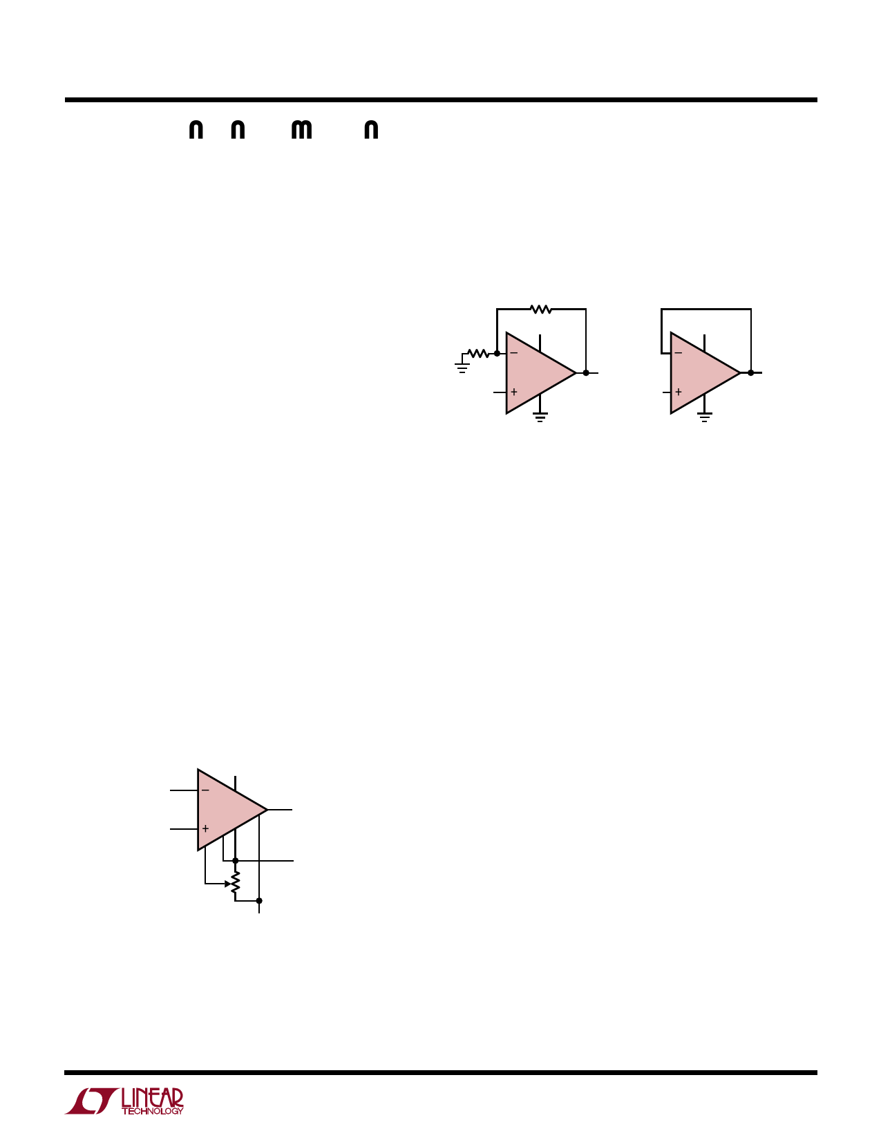
Output
The output voltage swing of the LT1635 is a function of
input overdrive as shown in the typical performance curves.
When monitoring voltages within 15mV of either rail, gain
should be taken to keep the output from saturating. For
example, a 1mV input signal will cause the amplifier to set
up in its linear region in the gain 100 configuration as
shown in Figure 2a. However, 1mV is not enough to make
the amplifier function properly in the voltage follower mode
(Figure 2b).
99R
5V
R–
LT1635
+OP AMP
1mV
5V
–
100mV
1mV
LT1635
+OP AMP
OUTPUT
SATURATED
≈ 2mV
1635 F02
(a)
(b)
Figure 2. Gain 100 Amplifier and Voltage Follower
Distortion
There are two main contributors of distortion in op amps:
distortion caused by nonlinear common mode rejection
and output crossover distortion as the output transitions
from sourcing to sinking current. The common mode
rejection ratio of the LT1635 is very good, typically 110dB.
Therefore, as long as the input operates in normal com-
mon mode range, there will be very little common mode
induced distortion. Crossover distortion will increase as
the output load resistance decreases. For the lowest dis-
tortion, the LT1635 should be operated with the output
always sourcing current.
Reference
The reference of the LT1635 consists of a 200mV precision
bandgap and a reference amplifier. As shown in the block
diagram, the 0.2V precision bandgap is referred to V – and
is internally connected to the noninverting input of the ref-
erence amplifier. This configuration offers great flexibility
in that the reference voltage can be amplified or the reference
amplifier can be used as a comparator. Unlike the op amp,
the output of the reference amplifier can only swing within
0.8V (typ) of the positive rail. To guarantee that the reference
amplifier does not saturate over the industrial temperature
range, the minimum operating supply should be 1.3V. The
reference amplifier can source 2mA of load current and can
sink 10µA over the industrial temperature range.
9
Share Link: 