ATMEGA48-15AZV 데이터 시트보기 (PDF) - Atmel Corporation
부품명
상세내역
제조사
ATMEGA48-15AZV Datasheet PDF : 340 Pages
| |||
Atmel ATmega48/88/168 Automotive
5.3.4
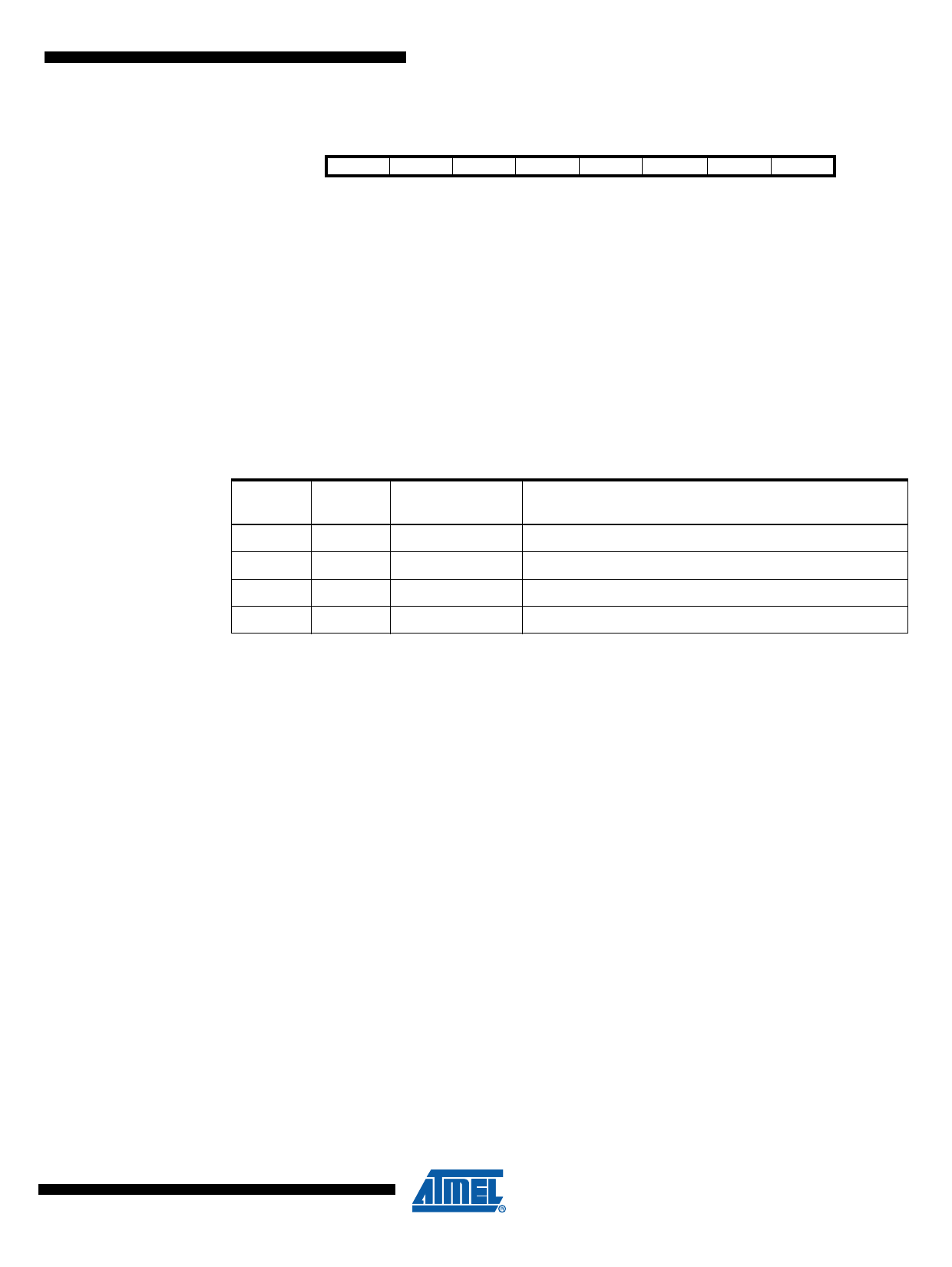
The EEPROM Control Register – EECR
Bit
7
6
–
–
Read/Write
R
R
Initial Value
0
0
5
EEPM1
R/W
X
4
EEPM0
R/W
X
3
EERIE
R/W
0
2
EEMPE
R/W
0
1
EEPE
R/W
X
0
EERE
R/W
0
• Bits 7..6 – Res: Reserved Bits
These bits are reserved bits in the ATmega48/88/168 and will always read as zero.
EECR
• Bits 5, 4 – EEPM1 and EEPM0: EEPROM Programming Mode Bits
The EEPROM Programming mode bit setting defines which programming action that will be trig-
gered when writing EEPE. It is possible to program data in one atomic operation (erase the old
value and program the new value) or to split the Erase and Write operations in two different
operations. The Programming times for the different modes are shown in Table 5-1. While EEPE
is set, any write to EEPMn will be ignored. During reset, the EEPMn bits will be reset to 0b00
unless the EEPROM is busy programming.
Table 5-1.
EEPM1
0
0
1
1
EEPROM Mode Bits
EEPM0
Programming
Time
0
3.4 ms
1
1.8 ms
0
1.8 ms
1
–
Operation
Erase and Write in one operation (Atomic Operation)
Erase Only
Write Only
Reserved for future use
• Bit 3 – EERIE: EEPROM Ready Interrupt Enable
Writing EERIE to one enables the EEPROM Ready Interrupt if the I bit in SREG is set. Writing
EERIE to zero disables the interrupt. The EEPROM Ready interrupt generates a constant inter-
rupt when EEPE is cleared.
• Bit 2 – EEMPE: EEPROM Master Write Enable
The EEMPE bit determines whether setting EEPE to one causes the EEPROM to be written.
When EEMPE is set, setting EEPE within four clock cycles will write data to the EEPROM at the
selected address If EEMPE is zero, setting EEPE will have no effect. When EEMPE has been
written to one by software, hardware clears the bit to zero after four clock cycles. See the
description of the EEPE bit for an EEPROM write procedure.
• Bit 1 – EEPE: EEPROM Write Enable
The EEPROM Write Enable Signal EEPE is the write strobe to the EEPROM. When address
and data are correctly set up, the EEPE bit must be written to one to write the value into the
EEPROM. The EEMPE bit must be written to one before a logical one is written to EEPE, other-
wise no EEPROM write takes place. The following procedure should be followed when writing
the EEPROM (the order of steps 3 and 4 is not essential):
1. Wait until EEPE becomes zero.
2. Wait until SELFPRGEN in SPMCSR becomes zero.
3. Write new EEPROM address to EEAR (optional).
4. Write new EEPROM data to EEDR (optional).
19
7530J–AVR–03/12
Share Link: 