72281L20PFG8 데이터 시트보기 (PDF) - Integrated Device Technology
부품명
상세내역
제조사
72281L20PFG8 Datasheet PDF : 26 Pages
| |||
IDT72281/72291
CMOS SuperSync FIFO™ 65,536 x 9 and 131,072 x 9
COMMERCIAL AND INDUSTRIAL
TEMPERATURE RANGES
AC ELECTRICAL CHARACTERISTICS(1)
(Commercial: VCC = 5V ± 10%, TA = 0°C to +70°C; Industrial: VCC = 5V ± 10%, TA = -40°C to +85°C)
Commercial
Commercial & Industrial(2)
Symbol
fS
Parameter
Clock Cycle Frequency
IDT72281L10
IDT72291L10
Min.
Max.
—
100
IDT72281L15
IDT72291L15
Min.
Max.
—
66.7
IDT72281L20
IDT72291L20
Min.
Max. Unit
—
50
MHz
tA
Data Access Time
2
6.5
2
10
2
12
ns
tCLK
Clock Cycle Time
10
—
15
—
20
—
ns
tCLKH
Clock High Time
4.5
—
6
—
8
—
ns
tCLKL
Clock Low Time
4.5
—
6
—
8
—
ns
tDS
Data Setup Time
3
—
4
—
5
—
ns
tDH
Data Hold Time
0
—
1
—
1
—
ns
tENS
Enable Setup Time
3
—
4
—
5
—
ns
tENH
Enable Hold Time
0
—
1
—
1
—
ns
tLDS
Load Setup Time
3
—
4
—
5
—
ns
tLDH
Load Hold Time
0
—
1
—
1
—
ns
tRS
Reset Pulse Width(3)
10
—
15
—
20
—
ns
tRSS
Reset Setup Time
10
—
15
—
20
—
ns
tRSR
Reset Recovery Time
10
—
15
—
20
—
ns
tRSF
Reset to Flag and Output Time
—
10
—
15
—
20
ns
tFWFT
Mode Select Time
0
—
0
—
0
—
ns
tRTS
Retransmit Setup Time
3
—
4
—
5
—
ns
tOLZ
Output Enable to Output in Low Z(4)
0
—
0
—
0
—
ns
tOE
Output Enable to Output Valid
2
6
3
8
3
10
ns
tOHZ
Output Enable to Output in High Z(4)
2
6
3
8
3
10
ns
tWFF
Write Clock to FF or IR
—
6.5
—
10
—
12
ns
tREF
Read Clock to EF or OR
—
6.5
—
10
—
12
ns
tPAF
Write Clock to PAF
—
6.5
—
10
—
12
ns
tPAE
Read Clock to PAE
—
6.5
—
10
—
12
ns
tHF
Clock to HF
—
16
—
20
—
22
ns
tSKEW1
Skew time between RCLK and WCLK for FF/IR
5
—
6
—
10
—
ns
tSKEW2
Skew time between RCLK and WCLK for PAE and PAF
12
—
15
—
20
—
ns
tSKEW3
Skew time between RCLK and WCLK for EF/OR
60
—
60
—
60
—
ns
NOTES:
1. All AC timings apply to both Standard IDT mode and First Word Fall Through mode.
2. Industrial temperature range product for 15ns and 20ns speed grade are available as a standard device.
3. Pulse widths less than minimum values are not allowed.
4. Values guaranteed by design, not currently tested.
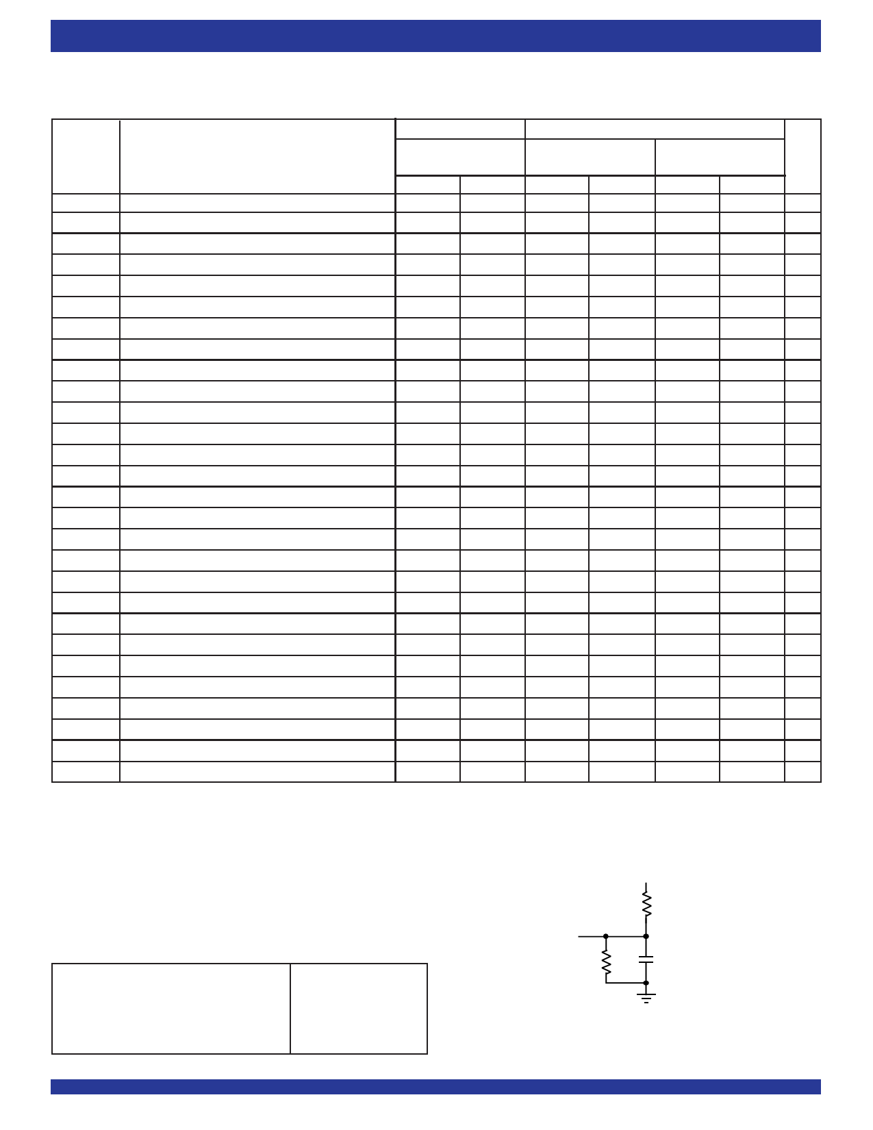
5V
1.1K
AC TEST CONDITIONS
Input Pulse Levels
Input Rise/Fall Times
Input Timing Reference Levels
Output Reference Levels
Output Load
GND to 3.0V
3ns
1.5V
1.5V
See Figure 2
D.U.T.
680Ω
30pF*
4675 drw 04
* Includes jig and scope capacitances.
Figure 2. Output Load
6
Share Link: 